Band gap engineering of atomically thin two-dimensional semiconductors*
Project supported by the National Natural Science Foundation of China (Grant Nos. 11374092, 61474040, 61574054, and 61505051), the Aid Program for Science and Technology Innovative Research Team in Higher Educational Institutions of Hunan Province, China, and the Science and Technology Department of Hunan Province, China (Grant No. 2014FJ2001).
Ge Cui-Huan, Li Hong-Lai, Zhu Xiao-Li ‡, Pan An-Lian †
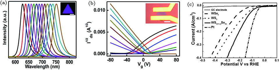
(color online) (a) Photoluminescence spectra of a series of composition tunable WSSe monolayer nanosheets. Inset: photoluminescence intensity mapping of the same WSSe nanosheets (x = 0.522; mapping peak is 687.5 nm; scale bar is 10 μm).[64] (b) Transfer characteristics (– plot) of WSSe nanosheet transistors with different S atomic ratios from nearly pure WSe (brown curve) to nearly pure WS (black curve).[64] (c) Polarization curves after iR correction obtained at a voltage sweeping rate of 5 mV in the monolayer WSSe (x = 0.43), monolayer WS, monolayer WSe, Pt and GC electrode.[62]