Band gap engineering of atomically thin two-dimensional semiconductors*
Project supported by the National Natural Science Foundation of China (Grant Nos. 11374092, 61474040, 61574054, and 61505051), the Aid Program for Science and Technology Innovative Research Team in Higher Educational Institutions of Hunan Province, China, and the Science and Technology Department of Hunan Province, China (Grant No. 2014FJ2001).
Ge Cui-Huan, Li Hong-Lai, Zhu Xiao-Li ‡, Pan An-Lian †
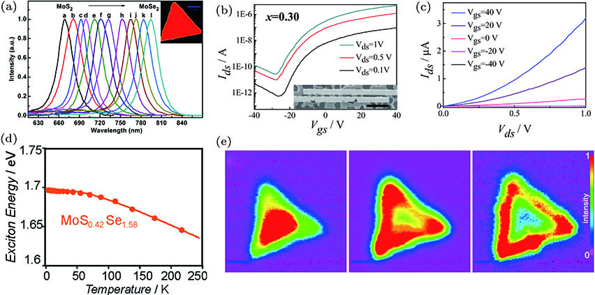
(color online) (a) PL spectrum of the complete composition MoSSe nanosheets and a typical PL mapping of a single ternary nanosheet (the inset, scale bar, 7 μm) excited with a 488 argon ion laser.[46] (b), (c) Source–drain current to the gate voltage () and the source–drain current to the source–drain voltage () for FETs containing the MoSSe monolayer for x = 0.30.[45] The inset shows the SEM image of the device channel. Scale bar is 5 μm. (d) The exciton emission energy as a function of the temperature of the monolayer alloy.[56] (e) Wavelength-dependent PL mapping of a single composition graded nanosheet alloy in the spectral regions of 680–690, 710–720, 750–760 nm, respectively (scale bars, 5 μm).[51]