Band gap engineering of atomically thin two-dimensional semiconductors*
Project supported by the National Natural Science Foundation of China (Grant Nos. 11374092, 61474040, 61574054, and 61505051), the Aid Program for Science and Technology Innovative Research Team in Higher Educational Institutions of Hunan Province, China, and the Science and Technology Department of Hunan Province, China (Grant No. 2014FJ2001).
Ge Cui-Huan, Li Hong-Lai, Zhu Xiao-Li ‡, Pan An-Lian †
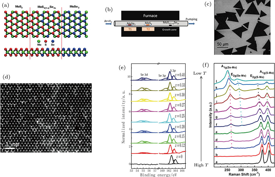
(color online) (a) Top and side views of the atomic structures of MoS2 (left), MoSSe alloy (middle), and MoSe (right) 2D TMDs. Note that the systems consist of three layers of atoms.[40] (b) Illustration of three-zone furnace for the growth of the MoSSe monolayer.[45] (c) Typical SEM morphology of the obtained ternary MoSSe nanosheets.[46] (d) ADF image of Se-doped MoS with ∼ 12% local Se concentration.[47] (e) XPS of all as-grown MoSSe monolayers.[45] (f) Raman spectrum of the MoSSe nanosheets excited with a 488 nm argon ion laser.[46]