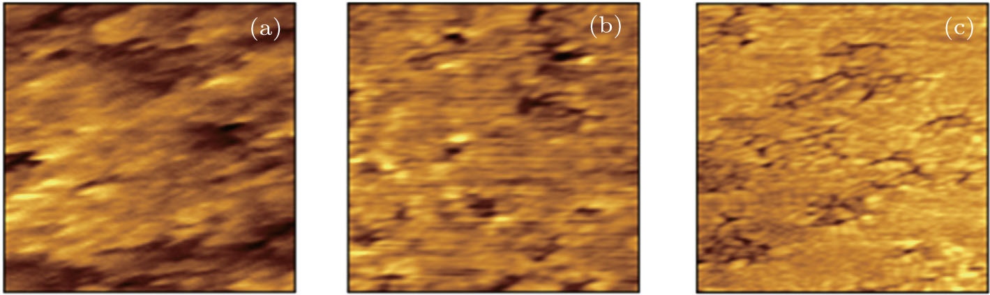
3. Results and discussionFigure 2 shows the typical AFM images with 5 μm × 5 μm scan area of the surfaces for three samples. The surface roughnesses in terms of root mean square (RMS) for samples A, B, and C are 0.65 nm, 0.93 nm, and 1.43 nm, respectively. It can be seen that the surface roughness is increased after treating Cl2 plasma, but the increment is no more than 0.3 nm indicating the low damage of the recess-gate. While compared with the surface roughness of sample A, that of sample C has increased 0.78 nm, which is related to greater RF power by oxygen plasma treatment.
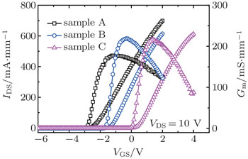
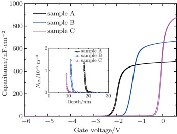
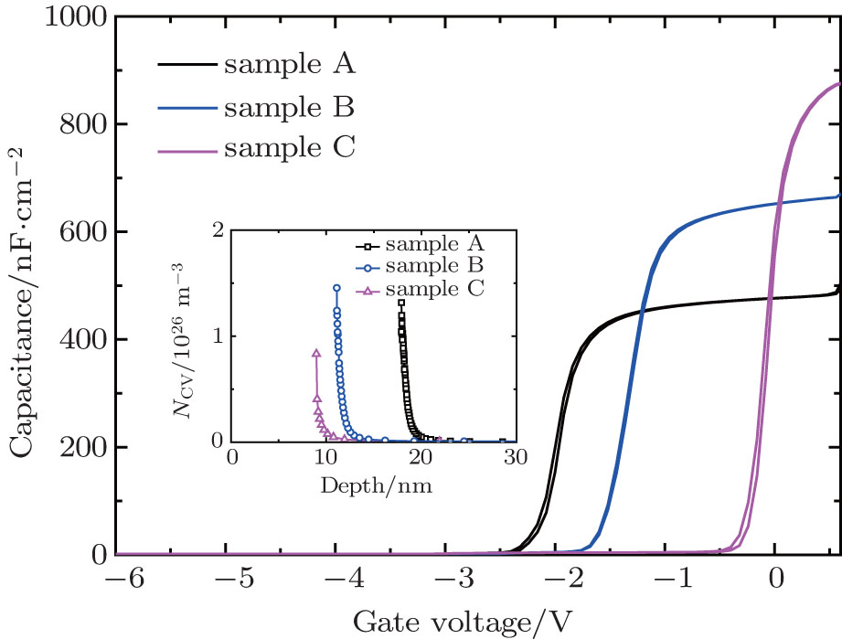
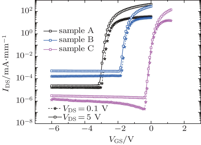
Figure 3 shows the typical transfer characteristics of three samples at VDS = 10 V. The threshold voltage (Vth) is defined as the gate bias intercept of the linear extrapolation of the drain current from the point of peak transconductance in transfer curves. The threshold voltage of sample A is about − 2.5 V and that of sample B is about − 1.2 V, that of sample C is 0.5 V. The AlGaN barrier layer thickness is reduced by etching, so the electron concentration in the channel is reduced.[7] The distribution of the carriers can be deduced from the capacitance–voltage (C–V) curves, as shown in Fig. 4. The AlGaN barrier layer thickness of sample A is 18 nm, that of sample B is 11 nm, and that of sample C is 9 nm. AlGaN barrier layer thickness under the gate region is reduced by 2 nm by oxygen plasma treatment. Therefore, the reduction of AlGaN barrier thickness is one of the reasons for the threshold voltage positive drift of sample C.
It can be seen that the channel current of sample C at VGS − Vth = 2 V is 410 mA/mm and that of sample B at VGS − Vth = 2 V is 420 mA/mm. It indicates that under the same gate drive voltage, two-dimensional electron gas (2DEG) concentration under the gate region after oxygen plasma treatment is not significantly changed, the current has little degradation. The peak transconductance of sample A is 177 mS/mm and that of sample B is 218 mS/mm. The higher peak transconductance of recess-gate HEMTs is related with the fact that the AlGaN barrier layer is thin under the gate region. Sample C shows the peak transconductance of 215 mS/mm, which indicates that the ability of gate control of HEMTs by oxygen plasma treatment is not significantly degraded.
Saito et al.[8] have studied the influence of the etching depth of recessed-gate on AlGaN/GaN HEMT characteristics. The relationship between the threshold voltage and AlGaN barrier layer thickness under the gate region can be expressed as


where
ED is the surface level at the AlGaN barrier layer, Δ
EC is the conduction band discontinuity,
N2D is the 2DEG density at the non-recessed region,
ϕB is the Schottky barrier height,
ε is the dielectric constant for the AlGaN layer,
tRA is the AlGaN layer thickness at the recessed region, and
tCR is the critical AlGaN barrier thickness while normalized 2DEG density is exactly equal to 0. Assuming
ED =
ϕB, the relationship between
Vth and
tRA is linear. The equation
Vth = 0.843–0.1857
tRA can be obtained by the calculation, the threshold voltage corresponding 9-nm AlGaN barrier layer should be − 0.82 V, however, the threshold voltage of 0.5 V is obtained with a 9-nm AlGaN barrier layer by oxygen plasma treatment. As a result, the threshold voltage positive drift has other factors.
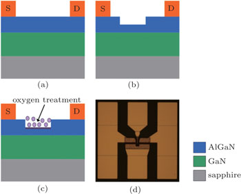
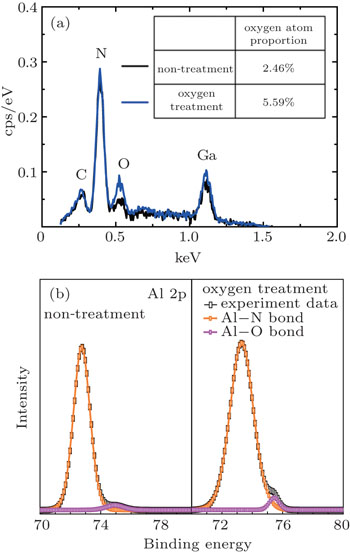
In order to study the mechanism for threshold voltage variations by oxygen plasma treatment, the SEM/EDS and XPS methods are used. The SEM/EDS method can be used to analyse the surface element changes, and XPS can scan and measure the chemical structure within 8 nm depth. Two specimens are obtained, one specimen has no treatment, and the other one is treated by oxygen plasma in the ICP system. The ICP coil power is 100 W, the RF power is 30 W, and the treatment time is 60 s. As shown in Fig. 5(a), the peaks of C, O, N, Ga can be seen in the non-treated specimen, the peak of element O appears due to the natural oxidation. After the oxygen plasma treatment, the peak intensity of O increases significantly and the percentage of oxygen atoms varies from 2.46% to 5.59% (more than doubled). Due to the presence of background noise and measurement errors, the peak intensity of Ga has a little change, the variation of Ga is low enough to be ignored. It can be inferred that, O2 and Al of the AlGaN barrier layer can be bonded. Figure 5(b) shows the XPS data of two specimens. As can be seen, the specimen without any treatment has an Al–N bond and Al–O bond, but the content of the Al–O bond is low, the formation of Al–O bond is related to the natural oxidation. However, compared with the specimen without treatment, the intensity of the Al–O bond in the specimen by oxygen plasma treatment is higher. This is proved that more Al element of AlGaN barrier layer in the specimen by oxygen plasma treatment can be oxidized, and the MIS structure can be formed.[9] This can reduce the content of Al component in the AlGaN barrier layer and further reduce the polarization effect of the barrier layer and deplete channel electrons.
Figure 6 shows the transfer characteristics of three samples under Semi-logarithmic coordinates system. The IDS of samples A and B are 10− 5 mA/mm and 10− 4 mA/mm in the off-state, respectively. However, the IDS of sample C is as low as 10− 6 mA/mm in the off-state, and the on/off current ratio of sample C is as high as 108. The off-state leakage current of sample B being larger than that of sample A may be due to the etching damage. Oxygen plasma treatment can reduce the content of the Al component in the AlGaN barrier layer and form the MIS structure, this can reduce 2DEG concentration under the gate region and the direct tunneling of electrons can be suppressed. So the off-state leakage current of sample C decreases two orders of magnitude than that of sample B.
When the device is biased at different drain voltage, the threshold voltage will drift due to the drain induced barrier lowering (DIBL) effect and the short channel effect. The rate of change of threshold voltage drift and drain-source voltage is usually used to measure the short channel effect.[10] It can be seen from Fig. 6, the DIBL of sample A is 37 mV/V, that of sample B is 16 mV/V, while the DIBL of sample C is 5 mV/V which is a small value. The small value of DIBL of sample C may be related to that the AlGaN barrier layer thickness is reduced and the ability of being gate-controlled is enhanced. In addition, it is noticed that the subthreshold swing (SS) of sample C is 80 mV/decade.
In order to study the influence of recessed gate etching and oxygen plasma treatment on the interface state, double sweep C–V curves at 100 kHz frequency of three samples are tested, as shown in Fig. 4. Due to the small area of devices' Schottky region, Schottky barrier diodes (SBDs) which have a larger Schottky region are selected. There is no obvious difference in hysteresis among three samples, indicating low concentration of surface states under the gate region by plasma treatment.[11] It is evident that a sharper rise is seen from the depletion mode to the accumulation mode obtained from sample C compared to that obtained on sample A. This indicates that, compared with sample A, sample C has less interface states and oxygen plasma treatment can effectively improve the interface quantity.[12]
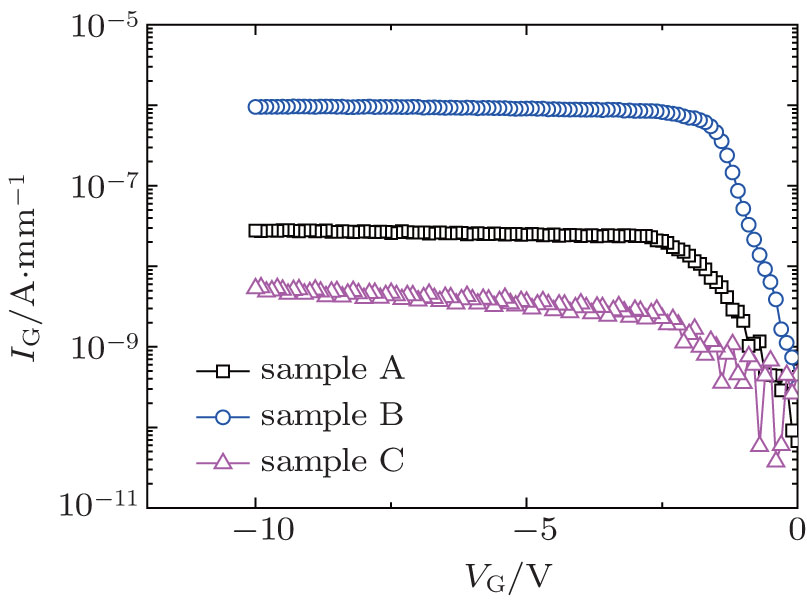
Figure 7 shows the Schottky reverse leakage current for three samples. The Schottky reverse leakage current of sample A reaches 10− 8 A/mm, and the Schottky reverse leakage current of sample B increases by an order of magnitude than that of sample A. However, the Schottky reverse leakage current of sample C is decreased by two orders of magnitude than that of sample B, reaching 10− 9 A/mm. There are three mechanisms for Schottky reverse leakage current.[13] The increase of the Schottky reverse leakage current of sample B mainly has two factors: one is the thin AlGaN barrier thickness increasing the probability of direct tunneling; the other is that the production of recessed gate brought a certain etching damage which could increase the probability of trap-assisted tunneling. However, by the C–V hysteresis curve, it can be observed that the surface states introduced by etching damage are very small. Therefore, the direct tunneling is the major factor for the Schottky reverse leakage current of the recessed gate device increasing. The thickness of the AlGaN barrier layer by oxygen plasma treatment can be further reduced, and the probability of direct tunneling increases further. However, the Schottky reverse leakage current of sample C is decreased by three orders of magnitude than that of sample B. It is attributed to the MIS layer which is formed on the surface of the AlGaN barrier by oxygen plasma treatment.
On the one hand, oxygen plasma treatment can make the Al composition in the AlGaN barrier layer reduce, and the electrons density below the gate is also decreased. On the other hand, the MIS layer can increase the barrier height that can suppress the probability of direct tunneling, and the oxygen plasma treatment does not introduce significant surface states. Therefore, the probability of trap-assisted tunneling is not possible, and the Schottky reverse leakage current by oxygen plasma treatment is suppressed.
Figure 8 shows the breakdown characteristics of three samples. In this paper, the drain bias which corresponds to the drain current reaching 1 mA/mm is considered to be the breakdown voltage. As can be seen from Fig. 8, there is little difference on the breakdown voltage between sample A and sample B, the breakdown voltage of them is about 160 V, which indicates that there is low damage in gate recess etching. After oxygen plasma treatment, due to the formation of the A–O bond, the MIS structure will be introduced between the gate and AlGaN barrier layer. The electron concentration of sample C decreases more significantly under the off-state condition and the Schottky reverse leakage current is reduced, the avalanche breakdown could be suppressed under the off-state condition. So the breakdown voltage of the sample C is larger than that of sample A and sample B.
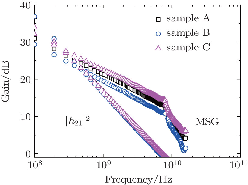
The on-wafer RF performance of three samples with LG = 1.2 μm is characterized from 100 MHz to 16 GHz. The current gain cutoff frequency (fT) is given by the extrapolation of |h21|2 with a − 20 dB/dec slope. The current gain and maximum stable gain (MSG) of three samples are derived from measured S parameters as a function of frequency, as shown in Fig. 9. For sample A, fT of 7 GHz and a power gain cutoff frequency (fmax) of 18 GHz are obtained at VDS = 10 V and VGS = − 1.3 V. For sample B, fT of 7.1 GHz and fmax of 17 GHz are obtained at VDS = 10 V and VGS = − 0.5 V. For sample C, fT of 7.3 GHz and fmax of 20 GHz are obtained at VDS = 10 V and VGS = 1.2 V. It can be seen that there are little differences on fT among three samples, fmax of sample C is the largest. fmax can be expressed as[14]
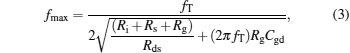
where
fT is the current-gain cutoff frequency and
Cgd is the gate-drain (depletion region) capacitance, while
Ri,
Rs,
Rg, and
Rds represent the gate-charging, source, gate, and output resistance, respectively. As known that
Rds is related to the short channel effect, good gate controlled ability leading the larger
Rds. After oxygen plasma treatment on the gate region, due to the combination of oxygen and Al such that the thickness of AlGaN barrier layer under the gate region is reduced. The gate controlled ability of sample C will be improved,
Rds will increase, so
fmax of sample C is increased.


 , Mi Min-Han1, Zheng Xue-Feng1, Zhang Meng2, Zhao Meng-Di1, Zhang Heng-Shuang1, Chen Li-Xiang2, Zhang Jin-Cheng1, Ma Xiao-Hua1, 2, Hao Yue1, 2]