Plasmon–phonon coupling in graphene–hyperbolic bilayer heterostructures
Yin Ge, Yuan Jun, Jiang Wei, Zhu Jianfei, Ma Yungui†,
State Key Laboratory of Modern Optical Instrumentation, Center for Optical and Electromagnetic Research, College of Optical Science and Engineering, Zhejiang University, Hangzhou 310058, China


† Corresponding author. E-mail: yungui@zju.edu.cn

Project supported by the National Natural Science Foundation of China (Grant No. 61271085) and the Natural Science Foundation of Zhejiang Province, China (Grant No. LR15F050001).

Abstract
Abstract

Polar dielectrics are important optical materials enabling the subwavelength manipulation of light in infrared due to their capability to excite phonon polaritons. In practice, it is highly desired to actively modify these hyperbolic phonon polaritons (HPPs) to optimize or tune the response of the device. In this work, we investigate the plasmonic material, a monolayer graphene, and study its hybrid structure with three kinds of hyperbolic thin films grown on SiO2 substrate. The inter-mode hybridization and their tunability have been thoroughly clarified from both the band dispersions and the mode patterns numerically calculated through a transfer matrix method. Our results show that these hybrid multilayer structures are of strong potentials for applications in plasmonic waveguides, modulators and detectors in infrared.

1. Introduction

Polar dielectric crystals can show hyperbolic dispersion characters in infrared arising from their ionic resonance driven by external electromagnetic (EM) fields, such as having anisotropic dielectric constants with sign difference.[1] On their surfaces with air, bounded phonon polaritons could be excited in the resonance state. Like hyperbolic metamaterials, light with large wavevectors or high energy density state can propagate inside these kinds of natural indefinite anisotropic materials.[2,3] Many interesting phenomena and related technological applications can be inspired by these special materials as subwavelength imaging,[4] sensing engineering,[5] or enhanced light radiation.[6] However, like plasmonic behaviors of noble metals in the visible regime,[7,8] it is hard to actively control or modify the EM properties of a hyperbolic dielectric once the device is fabricated. In practice, activity or tunable function is often desired in order to optimize or modulate the device performance, particularly when considering the narrow band phonon resonance nature of polar dielectrics. For this aim conductive materials with variable charge densities through optical pumping or electric doping have been adopted in the design of reconfigurable plasmonic devices.[9] Among them, graphene due to the relatively low damping loss and wideband response has attracted great attention as a key variable component, especially in the heterostructures of graphene–hexagonal boron nitride (hBN) composite in recent years.[10,11] Electron oscillations in graphene and ionic vibrations in polar dielectrics can produce plasmon–phonon hybrid modes. This hybrid structure, regarded as an advanced version of two-dimensional (2D) metamaterials, can absorb the virtues of both the hyperbolic dielectric and graphene by offering more freedoms to manipulate infrared waves and thus create new functional optical devices.[1214] It has been pointed out that graphene on a plasmonic dielectric substrate will possess larger carrier mobility than on a normal insulator such as SiO2.[15] In principle, reconfigurable plasmonic devices or functionalities in infrared can be anticipated applying this hybrid structure plus the additional features of low-loss and wideband.

In this work, we systematically investigated three kinds of graphene–hyperbolic heterostructures including graphene–hBN, graphene–aluminum nitride (AlN) and graphene–zinc oxide (ZnO), which all show strong electron–phonon coupling resonance in the mid-infrared regime. Among these hyperbolic components, hBN has attracted most attentions due to the low loss and high field confinement that are promising for subwavelength device applications.[16] Here, we give more comprehensive discussions on the field patterns and their propagation features associated with the hybrid coupling with graphene, especially when the properties of graphene are varied. For AlN and ZnO their semi-conductor and optoelectronics properties have been widely investigated in the field of material science,[17,18] while their EM characteristics on surface plasmon polartitons (SPPs), in particular hybridizing with another plasmonic layer are less discussed. It is scientifically and also practically instrumental to explore their optical features as potential plasmonic material candidates for novel photonic phenomena or functionalities.

For graphene–hBN heterostructure, we examine the hybrid polaritions in two different hyperbolic regions (Reststrahlen bands) and show that the propagation characteristics could be tuned by controlling the Fermi level. These two hyperbolic regions correspond to very different localized mode patterns. For the hybrid structure with AlN or ZnO constituent, which only has one hyperbolic resonance spectrum, our calculation shows that highly confined hybrid phonon–plasmonic modes could be achieved with proper damping parameters. Considering their optoelectronic properties, in particular for ZnO, more versatile or controlling features may be expected in a graphene–semiconductor hybrid system. Since the electric properties of the graphene layer can be vividly modified e.g., by applying a gate voltage[19] or optical pumping,[20] the hybrid plasmonic properties in principle could be tuned in both amplitude and wavelength. Hyperbolic responses of the polar crystals are usually narrow band and the hybrid combinations of different constituents proposed here may afford the options to realize the desired functionality in different spectrum regimes.

2. Theoretical model

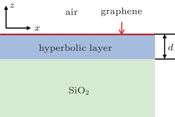
The multilayer hybrid topology investigated here is air/graphene/hyperbolic material (hBN, AlN, ZnO)/SiO2 substrate. The graphene layer we used is a monolayer sheet and treated as a 2D infinite material. The structure is infinite in the xy plane (Fig. 1) with the illumination of a p polarized plane wave. In Fig. 1, the middle grey region (−d < z < 0) represents the hyperbolic layer and the top (bottom) region is air (SiO2 substrate). Here we employ the standard transfer matrix method[21] to derive the reflection coefficient r of the hybrid structures. For our 2D structures the magnetic field along the y-axis direction can be expressed as

where the variable i = 1, 2, 3 stands for the region of air, hyperbolic layer, and SiO2, respectively. and are the wavevector components along the z and x axes, respectively. They satisfy the dispersion relation , where and are dielectric permittivity along the x and z axes, respectively. ai and bi are the coefficients of the incident and reflected waves, respectively. From the boundary continuity condition, we have the in-plane wavevector .

Fig. 1. Schematic of the hybrid structure in our calculation. The graphene monolayer (red) is sandwiched by top air and bottom hyperbolic layer (thickness d) grown on the SiO2 substrate. This two-dimensional composite structure is infinity along the y-axis direction.

The coefficients of the wave components in different regions are connected by a matrix equation

where the transfer matrix M is the product of three parts

In Eq. (3), M12 (M23) represents the interface transfer matrix between regions 1 and 2 (regions 2 and 3) and P12 represents the propagation matrix in region 2, i.e., the hyperbolic layer. These matrices can be deduced by Maxwell’s equations and boundary continuity conditions, defined by[21,22]

where d is the thickness of the hyperbolic layer, ɛ0 is vacuum permittivity, σ is the conductivity of graphene, and ω is angular frequency.

According to Eq. (2), we can calculate the reflection coefficient r = b1/a1. The eigenmode in a non-dissipative system will be excited for a vanishingly small incident wave (a1 ≈ 0). In this case the poles of r at real kx and ω give rise to the dispersion curve of the heterostructure.[16]

The conductivity σ of monolayer graphene in the infrared range is modeled using the local random phase approximation (RPA) expressed by[23,24]

where e is electron charge, ħ is reduced Planck constant, kB is Boltzmann constant, T is temperature, EF is the Fermi energy of graphene sheet, and τg is the electron relaxation time. The total conductivity σ is contributed by both interband (σinter) and intraband (σintra) conductions. The Fermi level of graphene layer can be tuned by many methods,[25] among which the most straightforward way is to apply a gate voltage. The electron relaxation time τg as a function of carrier mobility μ, Fermi energy EF, and Fermi velocity VF is written by . In calculation we use VF = 106 m/s and μ = 1000 cm2·V−1·s−1 for a low-doping graphene. Accordingly, EF = 0.5 eV and τg = 100 fs, which are used in the literature.[26] The dielectric properties of the SiO2 substrate are taken from Ref. [27]. According to these parameters the SiO2 substrate will also contribute a phonon resonance near 1130 cm−1, but which is neglected in our consideration due to its weak amplitude compared with the hyperbolic components of interest.

3. Results and discussion
3.1. With the hBN hyperbolic layer

Here the hyperbolic layer is assumed to be single crystal and the uniaxial direction is aligned parallel to the z-axis (Fig. 1). For hBN, the in-plane and out-of-plane dielectric functions can be described by the Lorentz model[28]

where ⊥(∥) represents the direction perpendicular (parallel) to the c-axis (or the z-axis in Fig. 1) of the optical crystal. The EM material parameters used in our calculation are given in Table 1. The calculated dispersions for hBN crystals are plotted in Fig. 2(a). As a typical Vander Waals crystal, hBN’s phonon resonances are anisotropic and have different eigenfrequencies for the in-plane and out-of-plane oscillations. As a consequence, it has two hyperbolic regions shown in Fig. 2(a), the type-I region with Re(ɛ) > 0 and Re(ɛ) < 0 in 780–830 cm−1 (shaded green) and the type-II region with Re(ɛ) < 0 and Re(ɛ) > 0 in 1370–1610 cm−1 (shaded orange). The real part of permittivity changes the sign in these two regions. In Fig. 2(b), we plot the hyperbolic isofrequency curves for these two bands at 800 cm−1 (left) and 1500 cm−1 (right), respectively. These straight dispersion features at high wavevectors corresponding to uniform group velocity vectors are very important for subwavelength lensing applications.[29] It is seen that at 800 cm−1 group and phase velocities of light traveling in hBN will propagate in the opposite directions, i.e., behaving as the back-forward wave.

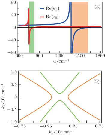
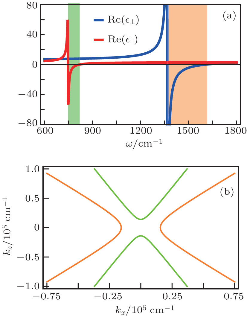
Fig. 2. Relative permittivity spectra (a) and isofrequency band dispersion (b) of hBN. The two shaded areas in panel (a) indicate the type I (green) and type II (orange) hyperbolic regions of hBN. Curves in panel (b) plot the corresponding isofrequency curves in these two regions at 800 cm−1 (green) and 1500 cm−1 (orange), respectively.
Table 1.

Material parameters used in our calculation. Here ɛ is the high frequency dielectric constant. ωLO and ωTO are the longitudinal-optic (LO) and transverse-optic (TO) phonon resonance frequencies, respectively. γLO and γTO are the damping constants of LO and TO phonon resonances, respectively. These parameters are obtained from the previous publications.[16,30,31]

.

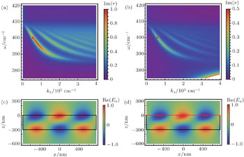
For the hybrid structure, we consider a 100-nm-thick hBN thin film as the hyperbolic layer. The resonant surface modes can be determined by the poles of the reflection coefficients and the mode dispersion patterns of the hybrid structure are obtained by plotting the imaginary part of the reflection coefficient r.[27,32] The results are given in Fig. 3 for the type-I region and in Fig. 4 for the type-II region. To better understand the mode characters, we also plot the field profiles of the modes at some frequency points as labeled in the dispersion patterns by dots. Figure 3(a) shows a monotonously increasing band curve for a free-standing graphene monolayer. The bounded mode pattern at 1700 cm−1 is plotted in Fig. 3(b) exhibiting a spatially symmetrical field distribution.

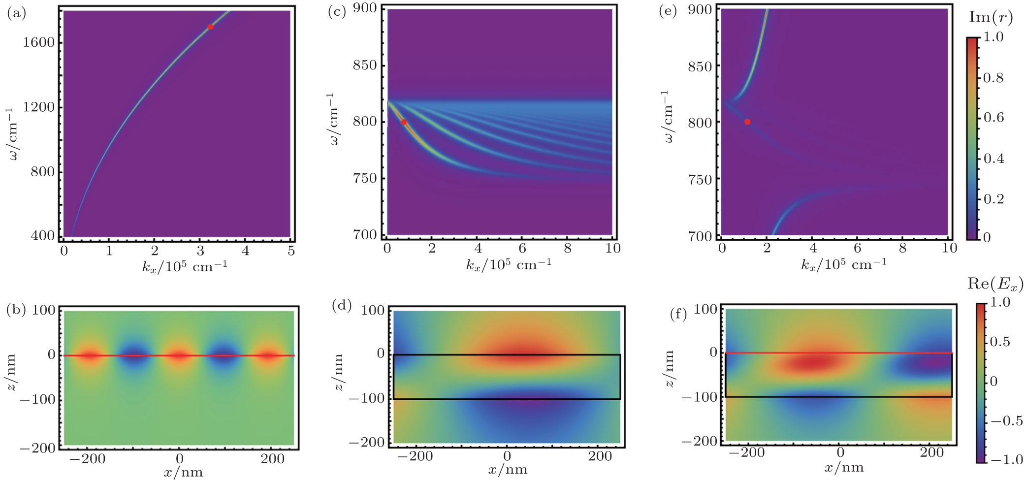
Fig. 3. Dispersions and field distributions of the modes for the free-standing graphene monolayer and the type-I band of the graphene–hBN heterostructure. The dispersions for (a) graphene (EF = 0.5 eV), (c) hBN and (e) their hybrid structure. (b), (d), (f). The field profiles of the modes of graphene, hBN and their hybrid structure at ω = 1700 cm−1, 800 cm−1, and 800 cm−1, respectively. The corresponding frequency positions in the left dispersion figures are indicated by red dots. The black lines in the field patterns profile the hyperbolic layer and the red line indicating the graphene sheet.
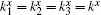
Fig. 4. Dispersions and mode patterns of the type-II band of the graphene–hBN heterostructures. The dispersion curves (a) without and (b) with graphene. The x-component electric field Ex distributions corresponding to the color points (c) C (1500 cm−1), (e) E (1600 cm−1), and (g) G (1500 cm−1) labeled in panel (a). The Ex distributions corresponding to the color points (d) D (1500 cm−1), (f) F (1600 cm−1), and (h) H (1700 cm−1) labeled in panel (b).

Figure 3(c) gives the dispersion diagram of the hBN film corresponding to the type-I band. Two distinct features are observed: (i) the Poynting vector S and the in-plane wavevector kx point towards opposite directions, which means that in this band the waves have negative phase velocity;[33] (ii) the first waveguide mode (node) has an integer index m = 1 which corresponds to an asymmetrical field distribution, for example as shown in Fig. 3(d). These two results are closely correlated to the hyperbolic dispersion features of the hBN constituent (see the green curve in Fig. 2(b)). More specifically, the minimum available value for the kz component of the hBN film determines the lowest order number of the waveguide modes. For the type-I band, it has a cutoff wavenumber starting from ω/c, while it has no such a limit for the type-II band. Thus, as shown in Figs. 4(a) and 4(d), the first waveguide mode for the type-II band has an integer index m = 0. Different index number m corresponds to different mode pattern, following the characteristic equation , where δ1 and δ2 are the reflection phase shifts of the top and bottom interface of the hyperbolic film, respectively.

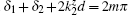
When covered by a graphene monolayer, as shown in Fig. 3(e), the dispersion branches of the hyperbolic film shift towards the right-hand. At ω = 800 cm−1, the momentum kx of the mode changes from 6.8 × 104 cm−1 to 10.2 × 104 cm−1, as denoted by the red dots in Figs. 3(c) and 3(e), meaning the reduction of the plasmon wavelength λp = 2π/kx. The mode field patterns are slightly modified as shown in Figs. 3(d) and 3(f). This wavelength can be calculated through the equation describing the poles of reflection coefficient. Neglecting high orders of kx for simplicity, one could have the change of plasmon wavelength Δλ induced by graphene.[13]

In Eq. (9), the graphene plasmon wavelength λg,p is approximately proportional to its Fermi energy and an external gate voltage may be applied to control the plasmon wavelength of the hybrid structure. But in this case, the near-field coupling between the localized modes of graphene and the hyperbolic layer is weak due to their mismatch in the field patterns, although they match in frequencies and wavenumbers. In this sense their existences effectively modify each other’s dielectric background rather than direct mode coupling.

For the type-II band, as shown in Fig. 4(a), the hyperbolic layer also possesses an infinite number of waveguide modes but with positive phase velocity. As addressed above, it takes the zero order waveguide mode (m = 0) as the first mode. The field distributions for the first two modes at 1500 cm−1 are plotted in Figs. 4(c) and 4(g), which show nearly symmetric and asymmetrical field patterns for these two modes, respectively. For the hybrid structure, the first hBN’s waveguide branch is smoothly coupled with the graphene mode (Fig. 4(b)) due to their common symmetric patterns. This trend is evidenced from the field patterns at the frequency points of 1500 cm−1 (Fig. 4(d)), 1600 cm−1 (Fig. 4(f)), and 1700 cm−1 (Fig. 4(h)), which show a mode transition from hBN’s waveguide to hybrid and then graphene’s SPP modes. Because graphene has a much wider SPP band, the frequency range for the hybrid mode is solely determined by the features of the hyperbolic layer. For the hybrid structure, the dispersion curve shifts towards left side compared with the pure hBN film. At ω = 1600 cm−1, the momentum kx changes from 6.56 × 105 cm−1 to 1.96 × 105 cm−1 after introducing the top graphene sheet.

In the above, we discuss the dispersion relationship with the real momentum kx. Generally when there exists material loss, this momentum should be a complex number with certain imaginary part κ. In the dispersion figures, the real and imaginary parts of the momentum correspond to the x-axis coordinate and the width of the bright lines, respectively.[16] Using numerical method (Lumerical Mode Solutions, with the same model and material parameters) to solve the eigenmode of the structure, we obtain the complex wavevectors at different Fermi energies for the free-standing graphene, as shown in Fig. 5(a). The loss in graphene can be controlled by increasing Fermi energy at high frequency. The real and imaginary wavevectors for a 100-nm-thick hBN film are plotted in Fig. 5(b), which shows strong loss at frequencies approaching ωLO. The dispersion curves of graphene–hBN heterostructure was plotted in Fig. 5(c) at different EF. With a small Fermi energy (EF = 0.1 eV), no hybrid mode exists in this band. The hybridized plasmon-phonon modes appear when EF is enhanced to 0.3 eV (blue) and 0.5 eV (green). Its wavelength shifts larger by raising the Fermi energy of graphene. The wavenumber of the bounded wave is significantly reduced due to the smooth transition from hBN’s lossy phonon resonance mode to graphene’s SPP mode which has a far smaller damping factor near ωLO. It is interestingly noted that the loss factor κ is effectively suppressed when hybridization happens, in particular at frequencies near ωLO.

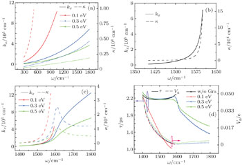
Fig. 5. Real (kx) and imaginary (κ) part momentums of the bounded modes in graphene (a), hBN (b) and the hybrid structure (c). Three different Fermi energy levels (EF = 0.1, 0.3, 0.5 eV) for graphene have been considered. (d) The life-time τ and group velocity Vg of the hybrid polaritons at different EF. The frequency ranges in panels (b) and (d) correspond to the type-II band of hBN.

In order to characterize the polariton propagation, the propagation velocities Vg (= dω/dk) and the decay time of HPPs τ (= L/Vg, L is the propagation length and equals 1/κ) are calculated at different EF. As shown in Fig. 5(d), the velocity is about one percent of light speed in vacuum. The propagation length is about tens of micrometers (not shown in the figure) and the decay time τ is about two picoseconds which is two orders larger than the ordinary plasmons in silver.[34] Due to this significant improvement in plasmon propagation length and lifetime, the highly confined low loss graphene–hBN heterostructure is promising as a core component in nanophotonic devices.

3.2. With the AlN hyperbolic layer

AlN is a wide band gap semiconductor, and has many important applications in high-efficiency optoelectronic and laser devices. It has the similar phonon resonance features with hBN, but characterized by different equation. In the multi-layer structure air/graphene/AlN/SiO2, the dielectric function of AlN layer is described by[30]

The parameters are given in Table 1. In our architecture, the c-axis of the AlN film is assumed to be in-plane aligned, which is experimentally achievable by epitaxial growth.[35] Both of the dielectric functions are Lorentz model for phonon crystals,[36] but AlN has a slight different from the hBN. AlN only has one hyperbolic region in 610–670 cm−1 as shown in Fig. 6(a) (shaded orange). When the frequency increases beyond the hyperbolic region, both the in-plane and out-of-plane permittivity become negative, which is different from the hBN case.

Fig. 6. Relative permittivity spectra of AlN (a) and ZnO (b). The c-axis of the crystals for AlN and ZnO is assumed to be in plane and out of plane, respectively. The dielectric functions of these two materials are described by Eq. (10). The hyperbolic regions are highlighted by the orange and green colors, respectively.

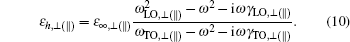
Using the same method described above, we calculate the dispersion relationship of the hybrid structure, shown in Figs. 7(a) and 7(b). The film thickness is set to be 200 nm. The damping constant of AlN is larger than hBN, which leads to relatively broader resonance line with less amplitude contrast. Here logarithmic scaling has been used for clear observing. For AlN, we observe different orders of HPP modes in the hyperbolic region (i.e., 610–670 cm−1), but only the lowest zero order is strong due to the loss issue. In addition, we also observe another dispersion curve corresponding to a metallic SPP-like mode above this hyperbolic region, where AlN is fully negative in permittivity. The two bright mode lines in Fig. 7(a) have asymptotic values about 820 cm−1 and 855 cm−1 at large wavenumber, whose field patterns are plotted in Figs. 7(c) and 7(e) at 800 cm−1 and 880 cm−1, respectively. The symmetrical waveguide and surface mode characteristics are clearly elaborated by these two figures. Here, the center of the zero order waveguide mode shifts closer to the bottom SiO2 side due to the asymmetry of the background dielectrics. It is interesting to see that the top SPP-like mode exhibits a negative slope for frequency above 855 cm−1 at large wavevectors, which may be used for applications such as slow waves.[37]

Fig. 7. Dispersions and mode patterns of the AlN and graphene-AlN. The dispersion curves (a) without and (b) with graphene. The Ex distributions corresponding to the color points (c) C (800 cm−1) and (e) E (880 cm−1) labeled in panel (a), and the Ex distributions corresponding to the color points (d) D (800 cm−1) and (f) F (950 cm−1) labeled in panel (b).

When a graphene layer is introduced on the top of the structure, both modes are modified due to their effective coupling with the SPP mode of graphene. After hybridization, the wavevector of the original lower waveguide mode is reduced. For example, the mode at 800 cm−1 shifts from 8.2 × 10⁻⁴ cm−1 to 5.2 × 10⁻⁴ cm−1 accompanied by a slight upward movement of the field distribution shown in Fig. 7(d). On the other side, the original SPP-like mode disappears at ω < 900 cm−1 and a new hybrid mode above 900 cm−1 comes out, shown in Fig. 7(b). Figure 7(f) plots the field distribution of this hybrid mode at 950 cm−1.

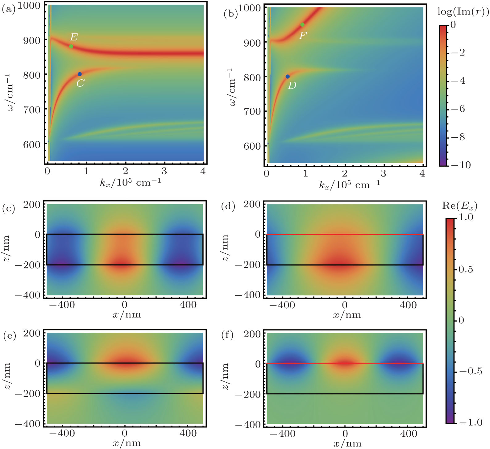
The influence of the material loss issues is investigated and the results are given in Figs. 8(a) and 8(b) without and with graphene, respectively. For the lower waveguide mode, the imaginary part of the mode wavevector is effectively suppressed by introducing a top graphene layer, in particular for the region near the resonance frequency ωLO, where κ has a nearly ten times reduction. This result is consistent with the results described above for the graphene–hBN hybrid. This is associated with the low loss properties of graphene in this frequency range.

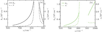
Fig. 8. Dispersion curves of graphene–AlN heterostructure with real and imaginary parts of wavevector, (a) without graphene and (b) with graphene. The Fermi energy EF is set to be 0.5 eV.
3.3. With the ZnO hyperbolic layer

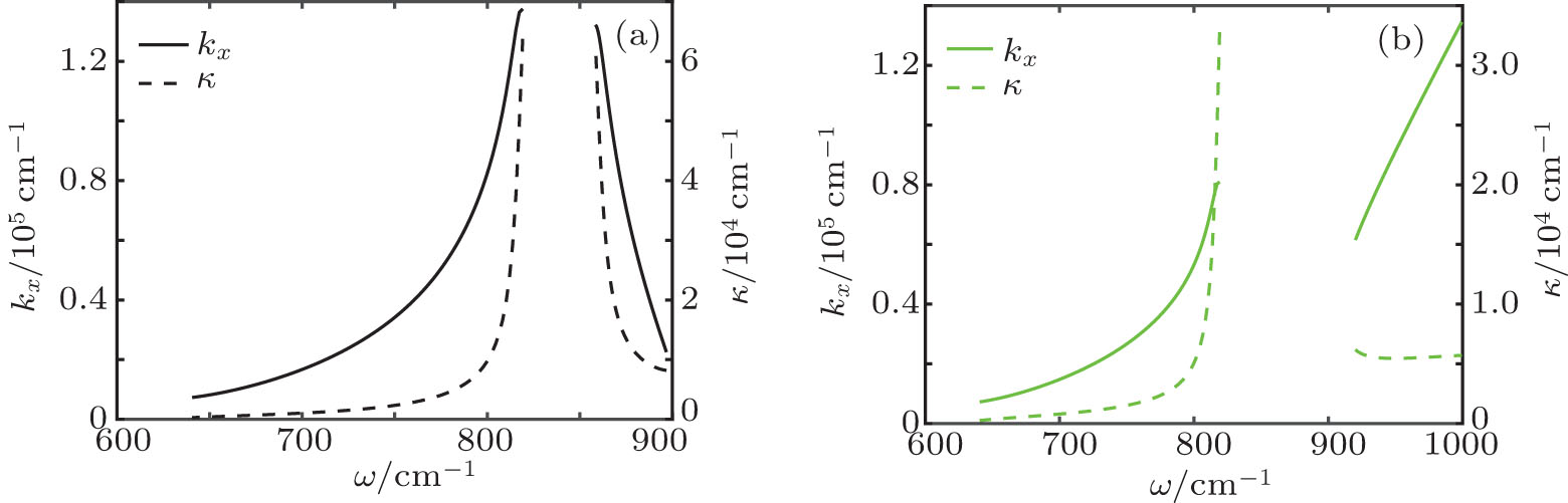
ZnO is a commonly used semiconductor sharing many properties with GaN and has been considered as a low-cost replacement to other materials for blue LEDs. Taking the free carriers and anisotropy into account, the dielectric function model of wurtzite ZnO can be expressed as the same as AlN.[31] However, we use a moderate damping constant when the single crystal ZnO is fabricated. In our calculation, the ZnO thickness is set to be 300 nm. In Figs. 9(a) and 9(b), we use a damping constant 3 to compute the dispersion curves. The band features are quite similar as those for the type-I band of the hBN film except that ZnO has a lower frequency band. Introduction of the graphene layer will change the dielectric background of the bounded modes and thus modify their dispersion. As example, it shifts from 6.8 × 104 cm−1 to 7.2 × 104 cm−1 at 400 cm−1. In addition, we found that if a larger damping constant is used (e.g., γ = 7), the high intensity curves become broader and the high order modes will disappear totally. The calculation shows that loss will be a key factor to influence the application of ZnO-based heterostructures. But for some specific applications such as thermal-radiation light source or thermophotovoltaic system, loss may be not a serious issue.

Fig. 9. Dispersions of graphene–ZnO heterostructure, (a) without graphene and (b) with graphene. (c), (d) The corresponding field profiles labeled by the red dots in panels (a) and (b) at ω = 400 cm−1, respectively.
4. Conclusion

We have studied the features of the HPPs and SPPs in graphene covered hyperbolic materials (hBN, AlN, and ZnO) based on the dispersion spectrum. hBN has the excellent property to form highly confined plasmons with low loss. In graphene–hBN heterostructure, hybrid polaritons combining the advantages of both constituents (i.e., low loss, tunability, wide band) have been illustrated. The phonon–polartiton resonances of wurtzite AlN and wurtzite ZnO covering different infrared frequencies have their own special applications. Besides controlling the Fermi energy of graphene, the loss in these materials can be also suppressed by improving the crystallographic qualities of the crystals. But it may not be an issue for applications such as light harvester or sensor. These hyperbolic materials supporting unique bulk waves are also useful for applications in subwavelength devices acting as spontaneous emission enhancement, super black-body thermal radiation,[38] and so on. Their electromagnetic coupling with a graphene monolayer gains more freedoms to modulate their functionalities, which is often highly desired for practical applications. Our results are meaningful for both scientific and practical purposes on the aspects of efficient subwavelength manipulation of infrared light.

Reference
1Poddubny AIorsh IBelov PKivshar Y 2013 Nat. Photonics 7 948
2Jacob Z 2014 Nat. Mater. 13 1081
3Noginov MLapine MPodolskiy VKivshar Y 2013 Opt. Express 21 14895
4Lu DLiu Z 2012 Nat. Commun. 3 1205
5Kabashin A VEvans PPastkovsky SHendren WWurtz G AAtkinson RPollard RPodolskiy V AZayats A V 2009 Nat. Mater. 8 867
6Poddubny A NBelov P AGinzburg PZayats A VKivshar Y S 2012 Phys. Rev. 86 035148
7High A ADevlin R CDibos APolking MWild D SPerczel Jde Leon N PLukin M DPark H 2015 Naure 522 192
8Monticone FAl‘u A 2014 Chin. Phys. 23 47809
9Ju LGeng BHorng JGirit CMartin MHao ZBechtel H ALiang XZettl AShen Y RWang F 2011 Nat. Nanotechnol. 6 630
10Kumar ALow TFung K HAvouris PFang N X 2015 Nano Lett. 15 3172
11Woessner ALundeberg M BGao YPrincipi AAlonso-Gonzaolez PCarrega MWatanabe KTaniguchi TVignale GPolini MHone JHillenbrand RKoppens F H L 2015 Nat. Mater. 14 421
12Caldwell J DVurgaftman ITischler J GGlembocki O JOwrutsky J CReinecke T L 2016 Nat. Nanotechnol. 11 9
13Dai SMa QLiu M KAndersen TFei ZGoldflam M DWagner MWatanabe KTaniguchi TThiemens M 2015 Nat. Nanotechnol. 10 682
14Zhang KZhang HCheng X 2016 Chin. Phys. 25 37104
15Dean C RYoung A FMeric ILee CWang LSorgenfrei SWatanabe KTaniguchi TKim PShepard K LHone J 2010 Nat. Nanotechnol. 5 722
16Dai SFei ZMa QRodin A SWagner MMcLeod A SLiu M KGannett WRegan WWatanabe KTaniguchi TThiemens MDominguez GCastro Neto A HZettl AKeilmann FJarillo-Herrero PFogler M MBasov D N 2014 Science 343 1125
17Taniyasu YKasu MMakimoto T 2006 Nature 441 325
18Lee S CNg S SAl-Hardan N HAbdullah M JHassan ZHassan H A 2011 Thin Solid Films 519 3703
19Carrasco ETamagnone MMosig J RLow TPerruisseau-Carrier J 2015 Nanotechnology 26 134002
20Wagner MFei ZMcLeod A SRodin A SBao WIwinski E GZhao ZGoldflam MLiu MDominguez GThiemens MFogler M MCastro Neto A HLau C NAmarie SKeilmann FBasov D N 2014 Nano Lett. 14 894
21Zhan TShi XDai YLiu XZi J 2013 J. Phys.-Condens. Mat. 25 215301
22Li Z YLin L L2003Phys. Rev. E4046607
23Xiang YGuo JDai XWen STang D 2014 Opt. Express 22 3054
24Zhang LZhang ZKang CCheng BChen LYang XWang JLi WWang B 2014 Opt. Express 22 14022
25Cheng HChen SYu PLiu WLi ZLi JXie BTian J 2015 Adv. Opt. Mater. 3 1744
26Messina RBen-Abdallah P 2013 Sci. Rep.-UK 3 1383
27Fei ZAndreev G OBao WZhang L MMcLeod A SWang CStewart MKZhao ZDominguez GThiemens MFogler MMTauber MJCastro-Neto A HLau C NKeilmann FBasov D N 2011 Nano Lett. 11 4701
28Cai YZhang LZeng QCheng LXu Y 2007 Solid State Commun. 141 262
29Dai SMa QAndersen TMcleod A SFei ZLiu M KWagner MWatanabe KTaniguchi TThiemens MKeilmann FJarillo-Herrero PFogler M MBasov D N 2015 Nat. Commun. 6 6963
30Ng S SOoi P KLee S CHassan ZAbu Hassan H 2012 Mater. Chem. Phys. 134 493
31Lee S CNg S SAbu Hassan HHassan ZDumelow T 2014 Thin Solid Films 551 114
32Biehs S ABen-Abdallah PRosa F SJoulain KGreffet J J 2011 Opt. Express 19 A1088
33Yoxall ESchnell MNikitin A YTxoperena OWoessner ALundeberg M BCasanova FHueso L EKoppens F H LHillenbrand R 2015 Nat. Photonics 9 674
34Naik G VShalaev V MBoltasseva A 2013 Adv. Mater. 25 3264
35Kao H LShih P JLai C H 1999 Jpn. J. Appl. Phys. 38 1526
36Dumelow TParker T JSmith S R PTilley D R 1993 Surf. Sci. Rep. 17 151
37Dionne J AVerhagen EPolman AAtwater H A 2008 Opt. Express 16 19001
38Guo YNewman WCortes C LJacob Z 2012 Adv. OptoElectron. 2012 1