1. IntroductionThe conventional metal-oxide-semiconductor field effect transistor (MOSFET) has entered the sub-20-nm stage and encountered more and more physical and technology limitations.[1,2] The artificial quantum dot made in MOSFET could exhibit quantum transport at room temperature.[3] When the effective gate length of silicon MOSFET is of the order of dozens of nanometers, the electrical properties of the device are no longer dependent on the average doping density but the distribution of individual dopant atoms in the channel. The random distribution of dopant atoms in the silicon nanowire, which act as quantum dots (QDs), will affect the electrical characteristics.[4–7] The scanning tunneling microscope (STM) with atomic resolution has been used to fabricate single dopant atom devices on a silicon surface terminated with hydrogens.[8] Further, the transport spectroscopy of a single dopant atom in an n–p–n silicon nanowire transistor has been investigated in recent years.[9,10] Compared with those in the inversion-mode transistor, carriers in the silicon junctionless nanowire transistor (JNT) flow in the middle of the nanowire instead of the surface inversion layer, which leads to more apparent quantum-confinement effect on the carrier transport.[11–15] At the initial stage of conduction, the carriers flow through a very narrow conductive path in the center of the nanowire. With the gate voltage increasing, the conductive path is gradually broadened until it forms a cross-section physically.[11] The electric field perpendicular to the current flow is lower in JNT than in a regular inversion-mode transistor. The electrons in JNT mainly flow through a bulk channel instead of a surface channel. Thus it can be seen that the surface roughness scattering has little influence on electron mobility. The more significant current oscillations could be observed in JNTs.[13] Therefore, it is very necessary to understand the influence of dopant atoms on the carrier transport behaviors in the variable conductive path of JNT.
In this work, we fabricate an n-type single-channel silicon JNT and experimentally investigate the electric-field-dependent charge delocalization from dopant atoms in a temperature range from 10 K to 250 K. Previously, Prati et al. observed the Anderson–Mott transition from the individual donor regime to the Hubbard band regime in silicon transistor doped with a few arsenic atoms.[16] More recently, Qiu et al. demonstrated the transport of few-layer molybdenum disulphide (MoS2) in low-carrier-density regime, which can be explained by hopping through defect-induced localized states.[17] Turk et al. investigated the gate dependence of charge delocalization below the mobility edge in a QD field effect transistor at low temperatures.[18] Roche et al. measured a large valley-orbit splitting for shallow isolated phosphorus donors in a silicon gated nanowire by using a double dopant transport spectroscopy.[19] Here we present the Arrhenius plot of the temperature-dependent conductance, which demonstrates that the electron transport behavior changes from variable-range hopping to nearest-neighbor hopping, at a transition temperature of 30 K. The activation energy for the charge delocalization, extracted from the Arrhenius plot, gradually decreases due to the confinement potential of the conduction channel decreasing from the threshold voltage to the flatband voltage. Furthermore, we find that the activation energy at the fixed gate voltage increases with increasing source–drain bias within a temperature range from 30 K to 100 K, but decreases above the temperature of 100 K.
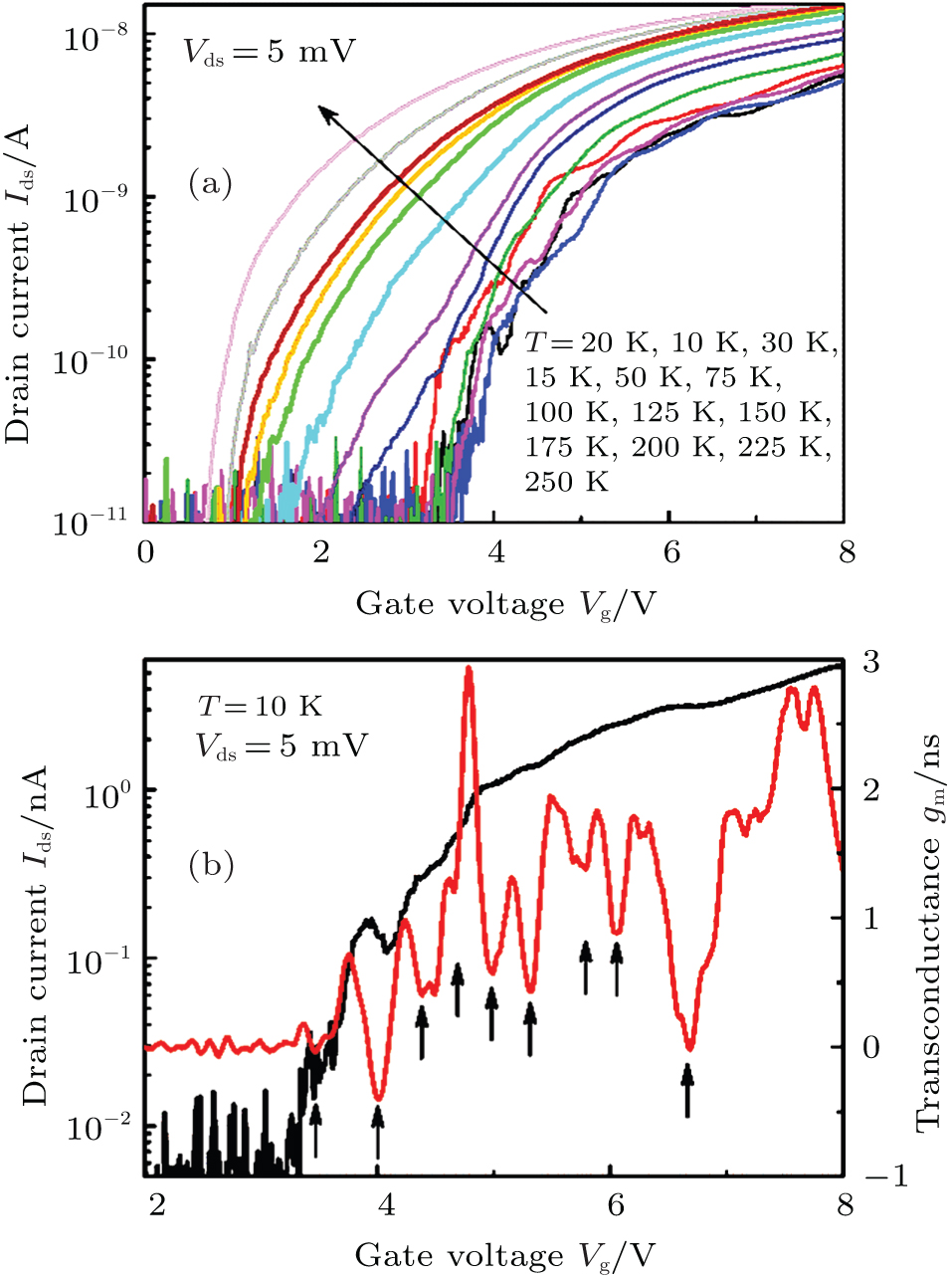
3. Results and discussionFigure 2(a) shows the variations of measured drain current Ids with gate voltage Vg in a temperature range from 10 K to 250 K at Vds = 5 mV. Clear drain current oscillations are observed below 100 K at the initial stage of the conduction, which is due to the electron tunneling through donor-induced QDs. When the JNT just begins to work, the cross section of the conductive channel is much smaller than the physics size of the silicon nanowire. A few dopants in the long conductive channel will notably affect electron transport at the initial stage.[4,20–22] With temperature increasing, the current oscillations gradually disappear under the influence of thermal energy.
Figure 2(b) illustrates the curve of drain-current peaks and transconductance oscillations with Vds = 5 mV at 10 K. The valleys of the transconductance curve correspond to the drain-current peaks, marked by arrows. According to the average gate-voltage spacing between the marked current peaks ΔVg = 340 mV, we estimate the gate capacitance Cg = e/ΔVg ≈ 0.47 aF. The radius of donor-induced QD is estimated to be 0.99 nm by the capacitance model of a sphere in front of wall C = 4πεrε0r (where C is the QD capacitance), where εr is the relative permittivity of silicon dioxide and ε0 is the vacuum dielectric constant. We notice that the intensity of drain current at a temperature of 15 K is comparable to that at 30 K, but the current intensity at a temperature of 20 K is lowest. This result indicates that the production of the ionized donors as the scattering centers is enhanced significantly in a temperature range from 15 K to 20 K, depending on the dopant implantation dose. The electron mobility decreases to a lowest value at the temperature of 20 K because of the interplay between thermal activation and impurity scattering.[23]
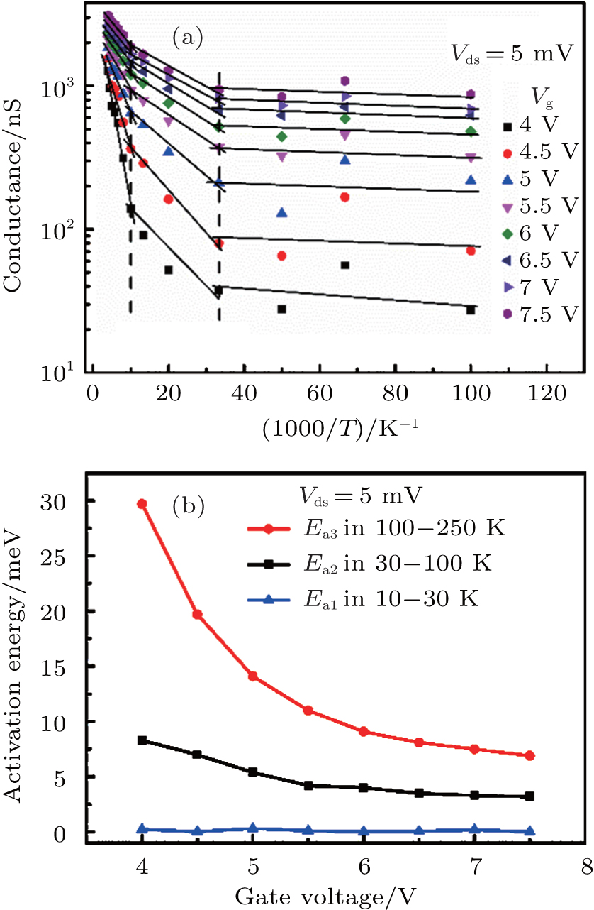
To obtain a better insight into the transport behaviors through the donor-induced QDs, the Arrhenius plot of the temperature-dependent conductance is shown in Fig. 3(a) at Vds = 5 mV with varying gate voltages. Clearly, the Arrhenius plot of the conductance shows three temperature regions, i.e., the lower temperature region (T < 30 K), the intermediate temperature region (30 K < T < 100 K), and the higher temperature region (100 K < T < 250 K). The gate-dependent activation energies are given by the temperature-dependent conductance G = A exp(−Ea/kBT) at a fixed gate voltage, where A is constant, kB is the Boltzmann constant, and Ea is the activation energy for electron hopping.[24,25] Figure 3(b) provides the curves of the activation energies Ea1, Ea2, and Ea3 versus gate voltage, which are extracted from the Arrhenius plots of the three temperature regions in Fig. 3(a). The activation energy for thermal electrons can be tuned with the help of the gate electric-field to make charge delocalized from dopant atoms.
In the lower temperature region (T < 30 K), the conductance is very weakly temperature-dependent due to the hopping electrons with the activation energy Ea1 less than 0.3 meV. Coulomb blockade and sequential tunneling through the donor-induced QDs are dominant. The activation energy Ea1 is independent of gate voltages only because the electron transport is dominated by varying-range electrons hopping with extremely low activation energy from one dopant atom to another. The density of the localized sites is very small as a Wigner-like system within the energy band so that the hopping electrons will not find the nearest neighbors but for those at the shortest hopping distance. Previously, we found that there exists an energy balance between the thermal activation and the Coulomb interaction at a critical temperature.[17] The transition temperature Tc has been derived from the balance condition to be Tc = 2.4e4ag0/kB(4πεrε0)2, where a is the localization length, g0 is the density of states at the Fermi energy, kB is the Boltzmann constant. The localization length a is estimated by using the QD radius of 0.99 nm. According to the implantation dose, the doping concentration ND is estimated to be 3 × 1018 cm−3. The mean distance between phosphorus donors is estimated to be  on a simple cubic lattice at the same density.[23] Then we can obtain the density of states g0 ≈ 8.7×10¹⁹ eV−1·cm−3 according to the activation energy of 8.3 meV at a gate voltage of 4.0 V, which is close to the voltage at the initial stage of the conduction. Using these parameters, we can obtain the transition temperature Tc of 37 K. The result is consistent with the experimental value of T2 = 30 K.
Above the critical temperature of transition from the melting of the Wigner-like system into the Fermi glass, thermally activated hopping transport is observed clearly with the increase of the drain current intensity in Fig. 2(a). With the help of the activation energy Ea2 above the temperature of 30 K, the electron localized in a neutral (D0) donor atom is able to be excited with the phonon-assistant energy to another already occupied neighbor donor atom. As a result, the coupling of negatively charged (D−) donor states gives rise to the upper Hubbard band.[24] With temperature increasing, the screening effect around each ionized donor will be increased due to the increase of the thermal electron density, which is identified by the negatively-shifted voltage at the onset current in Fig. 2(a). The Coulomb oscillations completely disappear above the temperature of 100 K. The excessive electrons will not be allowed to further occupy the negatively charged (D−) donor states in the upper Hubbard band. The thermal electrons with activation energy Ea3 are able to surmount the gate-induced potential energy between electrons and ionized donors, hopping from the lower Hubbard band of neutral (D0) donor states into the conduction band.
In addition, with the increase of temperatures, it is easy to observe in Fig. 3(b) that Ea3 is larger than Ea2 at a fixed gate voltage. The energy spacing between Ea3 and Ea2 could be considered as the charging energy from the lower to upper Hubbard bands in the dopant states. At the initial stage of the conduction (Vg = 4.0 V), the charging energy between the neutral (D0) states and the negatively charged (D−) states is 21.4 meV. With gate voltage increasing, the activation energies Ea2 and Ea3 gradually decrease and tend to be their corresponding stable values. The decrease of activation energy is ascribed to the decrease of confinement potential of the conduction channel and the lowest conduction levels moving to the flatband states, which are close to the source Fermi energy levels. The conductive path of JNTs would eventually expand into a physical cross-section as gate voltage reaches the flatband voltage.[9] The range of flatband voltage is estimated to be about 5.4 V–6.4 V within the temperature range from 10 K to 250 K according to the derivative of the transconductance as shown in Fig. 4.
The first peak is corresponding to the threshold voltage. Following the first peak in the dgm/dVg curve, the flat region is considered here as the flatband voltage because the gate control ability remains stable. The inset in Fig. 4 shows the extracted flatband voltages at different drain voltages and temperatures. The activation energy from the donor band to the conduction band tends to be a constant value when the gate voltage is close to the flatband voltage. According to Altermatt’s model,[22] the ionization energy of phosphorous donors in doped bulk silicon is estimated to be 22.75 meV from Edop = Edop,0/[1+(Ndop/Nref)2], where Edop,0 = 45.5 meV, Nref = 3×1018 cm−3, and Ndop = 3×1018 cm−3. The charge energy of 21.4 meV at an initial stage of the conduction (Vg = 4.0 V) is comparable to the ionization energy of donors in bulk silicon. Furthermore, the activation energies Ea3 and Ea2 reduce to 8.1 meV and 3.5 meV for the donors respectively in lower and upper Hubbard bands at flatband voltages (Vg = 6.5 V). This result indicates that the Hubbard bands are broadened with the increase of gate voltages so that the most energetic electrons at the band edge of localized states hop more easily into the bottom of the conduction band.
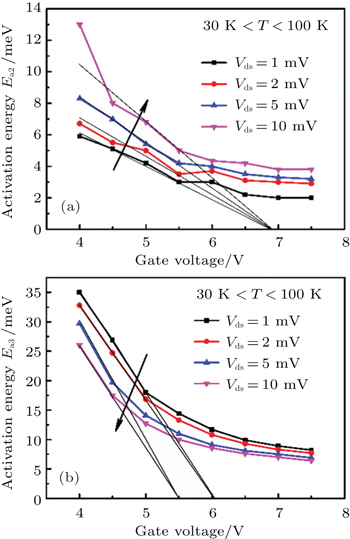
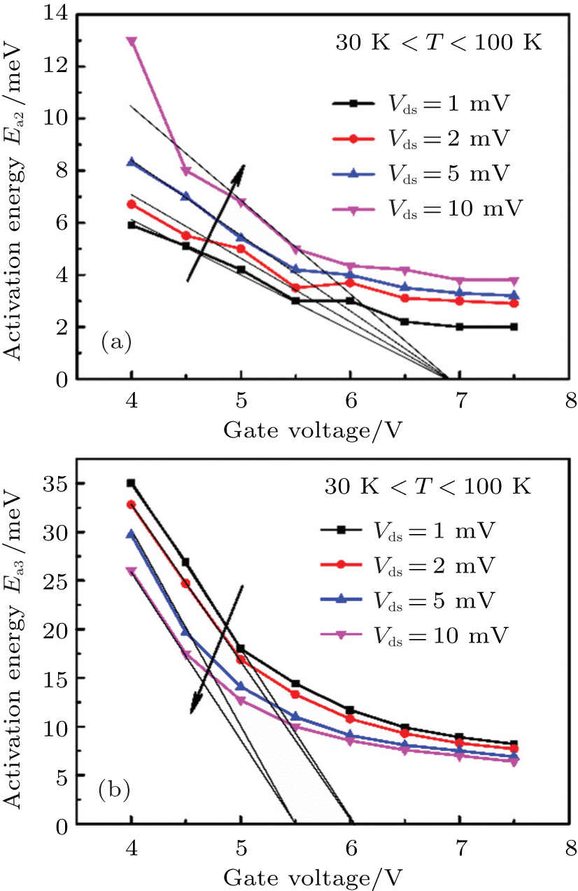
In addition to the influence of transverse electric field from gate voltage, the longitudinal electric field also has an effect on the transport behavior. The longitudinal electric field from the source–drain bias is along the silicon nanowire channel. Figures 5(a) and 5(b) show the curves of activation energies Ea2 and Ea3 each as a function of the gate voltage at the different source–drain bias voltages (Vds = 1 mV, 2 mV, 5 mV, and 10 mV), respectively. The extrapolations of the linear part to zero activation energy in Figs. 5(a) and 5(b) show that the conduction band edge EC in the channel reaches the Fermi energy EF at the gate voltages in a range of about 5.5 V–6.9 V,[4] which range agrees well with the flatband voltage range of about 5.4 V–6.4 V extracted from the derivative of the transconductance (dgm/dVg). We notice that the Ea2 in an energy range of 6 meV–13 meV at Vg = 4.0 V is comparable to Ea3 at the flatband voltage (Vg = 6.5 V), which is close to the thermal energy kBT = 8.7 meV at a temperature of 100 K. With increasing source–drain bias, the activation energy Ea2 in Fig. 5(a) increases at a fixed gate voltage within a temperature range from 30 K to 100 K, but Ea3 in Fig. 5(b) decreases above the temperature of 100 K. The significant difference probably results from the different temperature-dependent transport mechanisms.
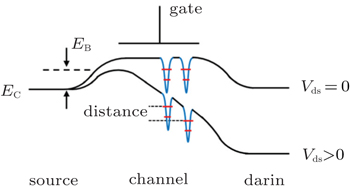
Figure 6 shows the schematic band diagrams of the device in longitudinal direction at different source–drain bias voltages. The conduction band edge profile with the localized states of donors and the gate-induced barrier potential is bent with broadening the Fermi level window between source and drain. The thermal electrons at extremely low temperatures (T < 30 K) could only hop between the equivalent energy levels, forming variable range hopping. With the gradual increase of temperature (30 K < T < 100 K), the thermal electrons can be excited near the Fermi energy with the help of phonons, forming nearest-neighbor hopping.[25] The discrete energy levels of ionized donors as QDs are degenerate in alignment as the source–drain bias is zero. With the increase of the source–drain bias, aligned energy levels shift. The spacing between misalignment QD levels is increased so that the conductive electrons require the phonon-assisted hopping with higher activation energies (Ea2) from one QD to another. As a result, the activation energy Ea2 near threshold voltage (Vg = 4.0 V) in Fig. 5(a) is very close to the thermal energy of about 8.7 meV at the temperature of 100 K, and Ea2 near flatband voltage (Vg = 6.5 V) is very close to the thermal energy of about 2.6 meV at the temperature of 30 K.
The gate-induced barrier height decreases with the increases of gate voltage and source–drain bias voltage, which can be reflected in Fig. 5(b) by the activation energy Ea3 at the temperatures above 100 K. Thermally activated transport is dominant in the higher temperature region. The electrons will gain enough thermal energy to surmount a gate-induced barrier and hop into the conduction channel. The gate-induced barrier potential is suppressed as the gate voltage increases to the flatband voltage. Therefore, the activation energy Ea3 near threshold voltage (Vg = 4.0 V) in Fig. 5(b) is very close to the thermal energy of about 21.7 meV at the temperature of 250 K, and Ea3 stable at the flatband voltage (Vg = 6.5 V) is very close to the thermal energy of about 8.7 meV at the temperature of 100 K. Furthermore, the electric field from the drain in the JNT with a gate length of 270 nm can reach through and lower the gate-induced barrier potential near the source. The effect of drain-induced barrier lowering (DIBL) results in the decrease of the activation energy Ea3 with the increase of source–drain bias.


 , Zhao Xiao-Song1, Zhang Wang1, Lyu Qi-Feng1, Ma Liu-Hong1, 2, Yang Fu-Hua1, 2, ‡,