1. IntroductionWith the rapid developments of satellite communication, radar and global positioning systems, it is required that the next-generation microwave ferrite devices will be smaller, self-biased and low loss.[1,2] In the centimeter wave range, yttrium iron garnet is an ideal candidate material for microwave ferrite devices due to its low microwave loss.[3] However, it needs a larger external magnetic field to obtain resonance in the millimeter wave region, which is a disadvantage for minimizing the size of the device. Barium ferrites (BaFe12O19, BaM) with excellent c-axis orientation each have a large uniaxial magnetocrystalline anisotropy field (∼17 kOe) and low microwave loss, so it is possible to provide enough biased magnetic field to produce resonance and eliminate the requirement for an external magnetic field, thus reducing the size of the device.[4] Hence, excellent c-axis orientation BaM thin film is a very attractive material for microwave ferrite devices in the millimeter wave region.
The structure of BaM can be described as RSR*S*, where R is the rhombohedral block including two O4-layers and one BaO3 layer with the composition  , and S is the spinel block formed by two O4-layers with the composition
  , where the asterisk means that the corresponding block has been turned 180 around the hexagonal c axis.[5] BaM has a hexagonal structure and its space group is P63/mmc.
So far, many methods have been tried to grow c-axis oriented BaM thin films, such as sputtering,[6] sol-gel,[7] metalloraganic decomposition,[8] liquid phase epitaxy,[9] etc. Besides these methods, pulsed laser deposition is another popular way to deposit BaM thin films.[10–12] In previous work, BaM thin films with high orientation and low microwave loss were deposited on sapphire substrate by pulsed laser deposition (PLD).[10,11] Our goal is to grow c-axis oriented BaM thin film with low microwave loss on silicon substrate for millimeter wave applications. Owing to the fact that the lattice mismatch between BaM and platinum (Pt) is small (about 5.8%),[13] we introduce Pt as the buffer layer in this research, and hopefully it can prevent Si from diffusing into BaM. In this paper, we discuss the effects of deposition substrate temperature on the microstructure, magnetic and microwave properties of BaM thin film.
2. ExperimentBaM thin films were deposited on Pt-coated silicon substrates. The target was of a conventionally sintered BaFe12O19 polycrystalline material. The target was ablated using a KrF (λ = 248 nm) excimer laser working at 10 Hz. The distance between target and substrate was 5 cm. The substrate temperature ranged from 850 °C to 925 °C, the oxygen pressure was in a range of 300 mTorr. After deposition, thin films were sintered in flowing oxygen for 2 h at a temperature of 1000 °C.
The ferromagnetic resonance (FMR) experiments were measured using short waveguide. In measurement, an external magnetic field which was perpendicular to the film plane was swept at a fixed frequency in a range from 30 GHz to 55 GHz. The microwave magnetic field was applied in the BaM thin film plane. Crystal structures of BaM films were measured by x-ray diffractometer (XRD, Bede TM 2000) with a Cu Kα radiation. Morphologies of films were carried out by atomic force microscopy (AFM). The M–H loops were measured by a vibration sample magnetometer (VSM) with an applied field in a range from −50 kOe to +50 kOe.
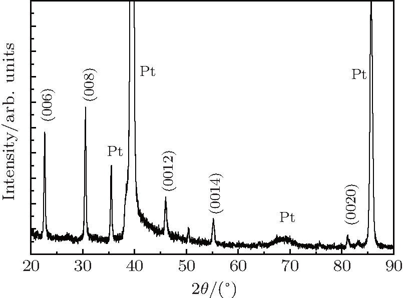
3. Results and discussionFigure 1 shows the typical XRD spectrum of BaM thin film which is deposited at a temperature of 910 °C and an oxygen pressure of 300 mTorr. It is clearly seen that all the diffractions are (00l) peaks, which means that the orientations of c-axis crystals are all in the direction perpendicular to the thin film plane. Except (00l) peaks of BaM, no other peak is detected, which indicates that the Pt can prevent the diffusion between Si and BaM. Hence, a pure BaM thin film can be obtained.
Since the degree of grain orientation (f) for thin film is very important for microwave loss, it needs to be calculated by the Lotgering way,[14] and it is expressed as

where
P denotes the ratio of the sum intensities of the (00/) and (
hkl) reflections for oriented sample, while the
P0 is that for the non-oriented one whose diffraction intensities are obtained from the randomly oriented powder. When substrate temperatures are 850, 880, 910, and 925 °C, the
f can be calculated to be 0.66, 0.82, 0.94, and 0.92, respectively. It is noted that the
f increases with increasing the substrate temperature, and reaches a maximum value (0.94) when the substrate temperature is 910 °C. This phenomenon means that 94% grains are perpendicular to thin film plane. It is proved that a higher
f leads to a low microwave loss (microwave loss is characterized by FMR linewith.
[15] The smaller the FMR linewith, the lower the microwave loss is), which will be further confirmed later in our paper.
The atomic force microscopy images (2 μm×2 μm) of BaM films deposited at 850 °C and 910 °C are shown in Figs. 2(a) and 2(b), respectively. From these two images, one can see more hexagonal grains lying in the film deposited at higher temperature. Many hexagonal crystals can be clearly observed in the thin film surface, further confirming that the orientation of the c axis is perpendicular to the thin film plane. It is also observed that the thin films have grain sizes ranging from 0.2 μm to 0.5 μm, which is very close to the single domain size.
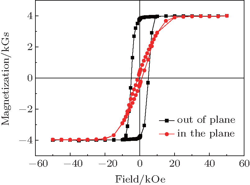
Figure 3 shows the hysteresis loops of BaM films deposited at 910 °C. The loops are measured with the applied external magnetic field that is in plane (IP) and perpendicular to plane (PTP) of thin film. It is clearly seen that the thin film has different hysteresis loops in the cases of IP and PTP, and saturated magnetization cannot be obtained in the case of IP because the applied magnetic field is less than the anisotropy field. This phenomenon indicates that each of these thin films has an anisotropic magnetic behavior, which is attributed to the preferred orientation of thin film grains. The saturated magnetization (Ms) of BaM is measured to be 4004 Gs. Hysteresis loops reveal that the squareness ratio (Mr/Ms) is as high as 0.93, which means that 93% of Ms remains after the external magnetic field has been withdrawn. Because the maximum magnetic field for our VSM measurement system is 12 kOe, which is less than the anisotropy field (HA) of BaM (∼17 kOe), we cannot obtain HA from our VSM measurement.
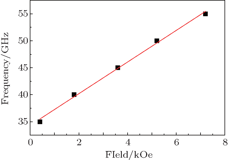
However, HA could be measured by FMR system. The relation between FMR frequency and external magnetic field is plotted in Fig. 4. In the measured range, the measured resonance dispersion obeys the following formula:[16]

where
f is the resonance frequency,
He is the external magnetic field,
HA is the anisotropy field, and
γ is the gyromagnetic ratio. By fitting the relation between FMR frequency and external magnetic field, we can obtain that
γ is equal to 2.8 GHz/kOe. Substituting the experimental data into Eq. (
2), we obtain
HA–4
πMs = 12.5 kOe. Thus,
HA can be calculated to be 16.5 kOe, which is reasonable when compared with the data (16.1 kOe) obtained from the VSM measurement.
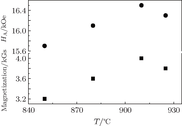
[15]The values of Ms and HA of the samples deposited in different substrate temperatures can also be obtained in the same way as that shown in Fig. 5. It is found that both Ms and HA increase with increasing substrate temperature, and reach their maximum values respectively when the substrate temperature is 910 °C; this variation trend is the same as the changing trend of f. This behavior means that the best f value and magnetic properties can be obtained when the substrate temperature is not too low nor too high. It is due to the fact that the good thermal energy leads to a better rearrangement in atoms mobility, which results in higher orientation and hence f and magnetic properties can be obtained.[17]
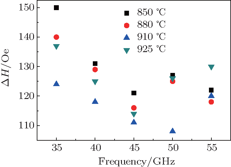
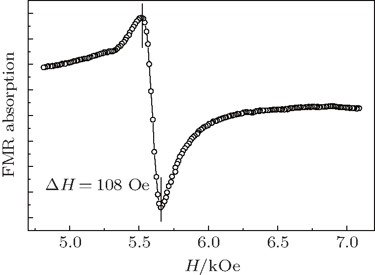
The plot of FMR line width (ΔH) versus frequency for the excellent thin film in a frequency range from 30 GHz to 55 GHz is shown in Fig. 6, and the FMR spectrum measured at 50 GHz is shown in Fig. 7. The ΔH is in a range from 100 Oe to 150 Oe, the smallest ΔH among the line widths of these thin films is measured to be 108 Oe at 50 GHz. These data are compared well with the values of those samples deposited on GaN/Al2O3 substrate.[10] These results show that this thin film has low microwave loss, making it have possible applications in microwave/millimeter wave devices.
4. ConclusionsHighly oriented BaM thin films are successfully deposited by PLD on Pt-coated Si wafer. It is found that the magnetic and microwave properties of BaM thin films are dependent on the substrate temperature: when the substrate temperature is 910 °C an excellent BaM film can be obtained which has a high c-axis orientation, high anisotropic field, and low microwave loss. A saturated magnetization of 4004 Gs, squareness ratio (Mr/Ms) of 0.93, and an anisotropy field of 16.5 kOe can be obtained for the excellent thin film, and the FMR line width is 108 Oe at 50 GHz. These properties indicate that this BaM thin film is suitable for applications in microwave/millimeter wave devices such as circulators, isolators, filters, etc.


 , Li Yuan-Xun2, Han Li-Kun2, Long Chao2, Zhang Huai-Wu2]