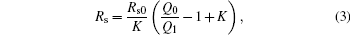
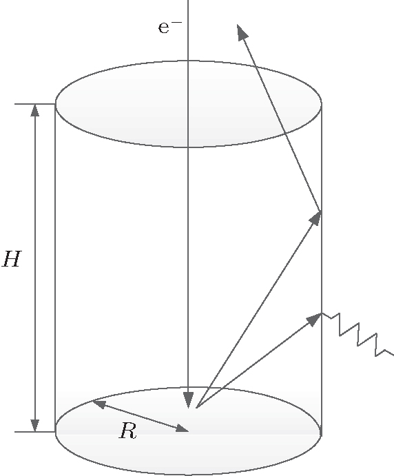
An efficient multipaction suppression method in microwave components for space application
Cui Wan-Zhao1, †, , Li Yun1, Yang Jing1, Hu Tian-Cun1, Wang Xin-Bo1, Wang Rui1, Zhang Na1, Zhang Hong-Tai1, He Yong-Ning2
National Key Laboratory of Science and Technology on Space Microwave, China Academy of Space Technology (Xi'an), Xi'an 710100, China
School of Electronic and Information Engineering, Xi'an Jiaotong University, Xi'an 710049, China


† Corresponding author. E-mail: cuiwanzhao@126.com

Project supported by the National Natural Science Foundation of China (Grant No. U1537211), the National Key Laboratory Key Foundation, China (Grant No. 9140C530101150C53011), and China Postdoctoral Science Foundation (Grant No. 2015M572661XB).

Abstract
Abstract

Multipaction, caused by the secondary electron emission phenomenon, has been a challenge in space applications due to the resulting degradation of system performance as well as the reduction in the service life of high power components. In this paper we report a novel approach to realize an effective increase in the multipaction threshold by employing micro-porous surfaces. Two micro-porous structures, i.e., a regular micro-porous array fabricated by photolithography pattern processing and an irregular micro-porous array fabricated by a direct chemical etching technique, are proposed for suppressing the secondary electron yield (SEY) and multipaction in components, and the benefits are validated both theoretically and experimentally. These surface processing technologies are compatible with the metal plating process, and offer substantial flexibility and accuracy in topology design. The suppression effect is quantified for the first time through the proper fitting of the surface morphology and the corresponding secondary emission properties. Insertion losses when using these structures decrease dramatically compared with regular millimeter-scale structures on high power dielectric windows. SEY tests on samples show that the maximum yield of Ag-plated samples is reduced from 2.17 to 1.58 for directly chemical etched samples. Multipaction testing of actual C-band impedance transformers shows that the discharge thresholds of the processed components increase from 2100 W to 5500 W for photolithography pattern processing and 7200 W for direct chemical etching, respectively. Insertion losses increase from 0.13 dB to only 0.15 dB for both surface treatments in the transmission band. The experimental results agree well with the simulation results, which offers great potential in the quantitative anti-multipaction design of high power microwave components for space applications.

PACS: 84.32.–y;52.40.Db;79.20.Ap
1. Introduction

Multipaction discharge resulting from the continual increase of secondary electrons due to the secondary electron emission (SEE) phenomenon[1,2] is a fundamental and influential phenomenon in many significant applications such as space thrusters, dusty plasma, high gradient accelerators, laser-plasma accelerators, high power lasers, and high power microwave (HPM) systems.[35] In recent years, with the wide spread of high power microwave components in space applications, multipaction issues have attracted increasing attention and have become an area of intense research.[68] Under particular field conditions involving frequency, field density, and phase at high power levels in a vacuum, multipaction discharge has become a bottle neck problem for spacecraft design,[9,10] causing signal deterioration, power dissipation, device damage, and even system failure. The secondary electron yield (SEY) refers to the average number of emitted electrons per incident primary electron, and is frequently used to characterize the SEE properties of a material. Owing to the volume and weight limitations of space vehicles, multipaction suppression remains a key challenge to payload system design.

One of the most effective means of suppressing SEY is to select material with a low SEY, which is determined by the crystalline structure and surface properties. Joy's database,[11] which includes SEY data for many materials, may be of great assistance for selecting low SEY coating materials. However, this suppression strategy is not always appropriate due to a lack of stability and, in particular, extreme requirements that may be imposed by the overall system performance in space.

In recent years, materials with artificial surface structures have been proposed for suppressing the SEY. In 2008, Pivi et al. verified that a grooved surface was effective for reducing the SEY over an energy range from tens of eV to several thousands of eV.[12] Then, from 2009 to 2011, Chang et al. investigated the feasibilities of employing periodic millimeter-scale rectangular and triangular profiles on dielectrics for suppressing the multipaction.[13,14] However, these surface structures may not be used in microwave components directly because the dimensions of the periodic structures are sufficiently large to affect the field distribution within microwave components, and thus causing large insertion losses. Based on our previous work, micrometer-scaled rectangular and triangular porous structures have been proposed for suppressing the SEE on metal samples, and the method was validated by the Monte Carlo method.[15] However, a corresponding multipaction suppression method for microwave components is still lacking.

In this paper, we report that the multipaction threshold of actual components is increased using micro-porous surfaces with a periodic cylindrical profile. Compared with rectangular and triangular structures, the proposed profile shows a better SEY suppression effect and offers feasible fabrication on device surface. Photolithography processing and the direct chemical etching technique are proposed for the surface treatments, which are not only compatible with component processing techniques, but also allows large size and uniform processing. A quantitative relationship between the variations of the SEY and the multipaction threshold for actual device is established through electromagnetic particle-in-cell (EM-PIC) simulation. The simulation and experimental results demonstrate that the entire physical process can be simulated and the suppression effect can be quantified, which offers great potential in the anti-multipaction design of high power microwave components.

2. SEY suppression by micro-porous surfaces on silver coatings
2.1. Theory model of the porous surface

Figure 1 illustrates the schematic model of the SEY suppression method using a micro-porous surface. The regular and non-regular structures artificially constructed on the metal surface are approximated by cylindrical wells and are defined by three primary parameters, e.g., the well radius R, the well depth H, and the distance between adjacent wells D. The figure indicates that the electron trajectory in a single well is bent and multi-generation electrons can be absorbed by the well.

Fig. 1. A schematic diagram of the SEY suppression method using a micro-porous surface characterized by a cylinder of height H and radius R.

When the radius of the well R is far smaller than the wavelength of the propagating wave λ, i.e., Rλ, the electron uniformly moves to the wall of the well while the electromagnetic wave can be neglected in the well. Based on the Monte Carlo method and a phenomenological statistical model of the SEY, electron trajectories can be tracked, and the emission probability from the well can be calculated. Then, the SEY of the well is calculated and defined as δw. Combined with the SEY of the flat surface, δf, the SEY of the micro-porous surface is given by

where P is the average distribution probability of the pores, which can be defined by the ratio between the porous surface area and the total surface area.

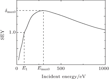
Through the Monte Carlo simulation with the cylinder well model of certain height and radius,[15] the SEY according to different incident energies and angles are recorded. The actual maximum yield δmax0 of the porous cylindrical surface is fitted by the function

where AR is the height-to-width ratio of the cylinder well and is given as AR = H/2R.

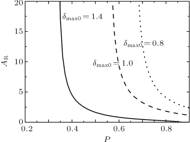
Thus, micro-porous structures can be designed to obtain a maximum decrease of the SEY as shown in Fig. 2.

Fig. 2. Variations of maximum yield of porous surfaces with porosity P and height-to-width ratios AR.

It can be concluded from Fig. 2 that the deeper and denser the pores, the smaller the maximum SEY is. Correspondingly, these pores on the surface are likely to suppress multipaction in microwave components due to the correlation between SEY and multipaction. Artificial structure such as the grooved surface is no longer applicable for microwave components due to the change of the electric performance. Furthermore, the increase of insertion loss due to the roughening of the surface is another challenge that should be suppressed for practical components.

At first, micro-cylindrical structures scaled from nanometer to micrometer on the metal surfaces are proposed for multipaction suppression when applying a field with the wavelength of centimeter scale (f = 300 MHz∼ 30 GHz). The secondary electrons are efficiently trapped in the well and it is conjectured that the insertion loss of the component increases little while R < 0.0001λ. For the approximation calculation of the loss due to the micro-structures, a resonant cavity is utilized and its quality factor, Q0, is measured. Replacing the top plate with one of a porous surface, the surface impedance is calculated from

where Rs0 is the surface impedance, K the dimension factor of the cavity, Q0 the quality factor of the initial resonant cavity, Q1 is the quality factor of the cavity with the porous top plate and Rs is the approximate surface impedance of the metal with porous surface.

Moreover, the photolithography pattern method and the directly chemical etching method are proposed for the surface treatment. The dielectric loss caused by plating dielectric foam on the metal is avoided.

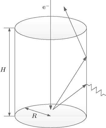
2.2. Design and fabrication of the porous surface

Regular and irregular micro-porous surfaces are fabricated on Ag-plated aluminum samples for validating the SEY suppression method. The regular surfaces are realized with a predefined shape using a traditional photolithography pattern process, and the direct chemical etching method is used for realizing the irregular micro-porous surfaces.[15]

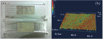
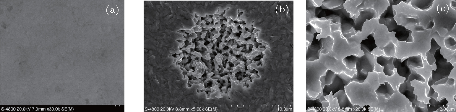
All Ag-plated samples are initially ultrasonically cleaned to remove dust and contamination. Figure 3 shows scanning electron microscopy (SEM) images of three different types of samples, i.e., the original flat Ag-coated sample, the photolithography pattern processed sample, and the directly chemical etched samples. A group of samples with irregular micro-pore arrays using ferric nitrate (Tianjin Yongsheng Fine Chemical Co., Tianjin, China, analytical reagents) in an aqueous solution with a mass fraction of 20% for tens of seconds at 50 °C and another group of samples with regular micro-pore arrays using traditional photolithography are fabricated. The parameters characterizing the physical micro-structures of the pores are measured and recorded in Tables 1 and 2.

Fig. 3. SEM images of samples with different surface treatments: (a) Ag-coated; (b) photolithography patterned; (c) directly chemical etched.
Table 1.

SEY of samples under different conditions of photolithography pattern.

.
Table 2.

SEY of samples under different etching conditions.

.

Correspondingly, it is reasonable to obtain the following conclusions:

Using theoretical analysis and calculation, the micro-structures on the metal surface can be ‘designed’ to suppress the secondary electron emission phenomenon and the suppression effect is quantified for the first time.

It should be noted that the plating thickness of silver is 10 μm which is thick enough to guarantee that the aluminum base is not naked after the surface treatment processing.

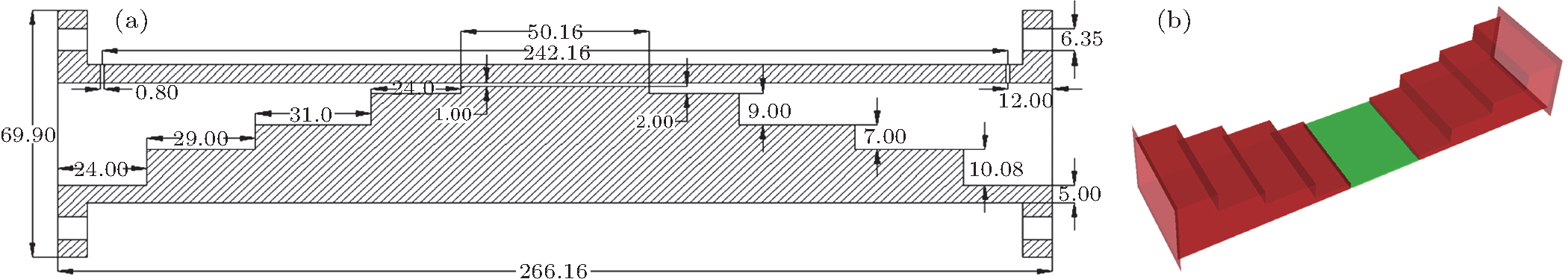
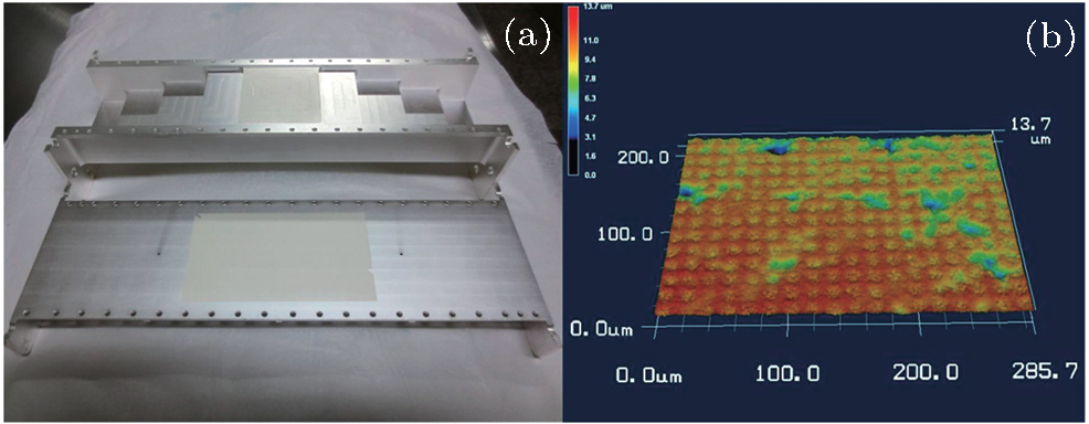
2.3. SEY and multipaction suppression in practical components

Fabrication of a porous surface on the practical components brought a new challenge to the surface treatment technology compared with that on the samples. Corners, steps, bent and wedged waveguides made it difficult to construct a uniform porous surface with a predesigned size. In addition, the large physical sizes of practical components exacerbate the problem. To solve these problems, some practical efforts have been made. On the one hand, the spin processor (Chemat Technology, Spin Master 100) burdened larger load is utilized for the photolithography patterned processing and the etching method is optimized. On the other hand, the electromagnetic analysis is performed on the components to find the sensitive area where the field density is strongest and multipaction is most likely to occur.

Parameter optimization shows that larger P and AR lead to a better SEY suppression effect. To obtain a compromise between processing limitations and parameter optimization in practice, samples with diameters of about 20 μm and depths of about 8 μm were chosen for multipaction suppression in metal components.

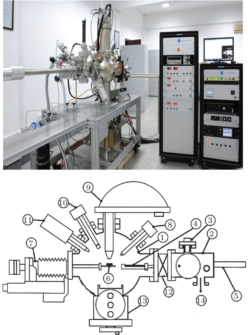
The total SEY consists of two different populations: the true secondary electrons and the backscattered secondary electrons. We measure the SEY using the conventional sample-current method.[16] The SEY measurement is conducted by the apparatus shown in Fig. 4. The measurement apparatus is comprised of three major systems: ultra-high vacuum chamber, test system, and data processing system.[16,17] The test system is composed of a low energy electron gun, sample platform, and pico-ammeter. The electron gun is a thermionic electron gun, which is integrated in the electron spectrometer (DESA150, Staib Instruments, Germany).

Fig. 4. Configuration of the SEY measurement platform, 1: analysis chamber; 2: loading chamber; 3: sample plate entry; 4: sample transfer plate; 5: rack and pinion transfer mechanism; 6: sample plate travel; 7: four-dimensional manipulator; 8: ion gun; 9: electrostatic energy analyzer; 10: electron gun; 11: residual gas analyzer; 12: gate valve; 13: ion pump and Ti sublimation pump; 14: molecule pump and mechanical pump.

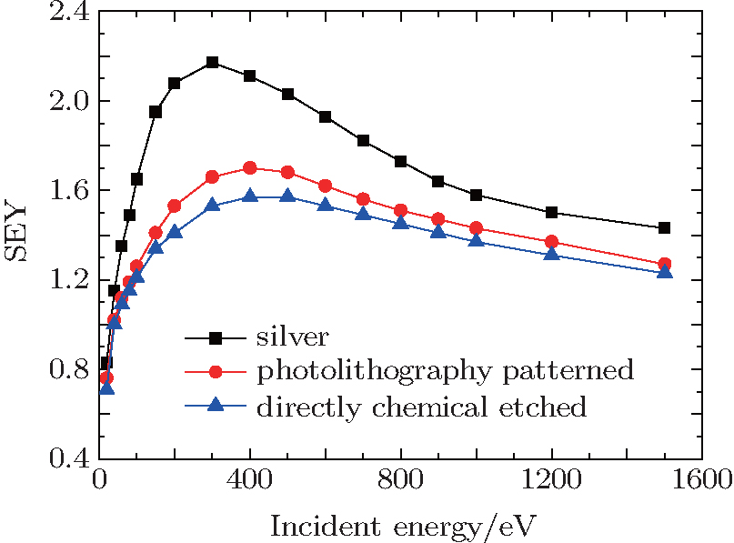
The SEY test results of witness samples of practical components are shown in Fig. 5. The largest feasibly obtainable porosity on the components is about 57%. It can be seen that the curves of the photolithography patterned and directly chemical etched sample surfaces demonstrate a good SEY suppression effect over the entire energy range considered. The directly chemical etched sample achieves the smallest SEY. This type of micro-structured surface and etching method can be extended to the SEY suppressions of other metals. Thus, the micro-porous surface offers an alternative approach to SEY suppression in relevant areas such as multipaction effects in satellite payloads and electron cloud effects in accelerators.

Fig. 5. The SEY characteristics of three different types of surfaces on practical components.
3. Simulation and experimental validation of multipaction suppression

In our previous work, we proposed a self-consistent EM-PIC algorithm for multipaction simulation and analysis.[18,19] Compared with analytical methods[20,21] or other simulation tools[2225] such as the multipactor calculator by the European Space Agency (ESA),[20] our method of analyzing the multipaction threshold demonstrates a remarkable advantage. The three-dimensional electron and the field dynamics of multipaction can be repeated, and the threshold is predicted by using the EM-PIC method.

3.1. SEY curve fit for multipaction simulation

Based on the theoretical analysis, the physical dimensions of micro-pores on the surface are designed to realize the optimal suppression effect of SEY in practical components. However, the calculated SEE parameters are not accurate enough for the multipaction simulation nor for threshold analysis neither. Thus, combining with the practical SEY properties of material with concrete morphology,[26,27] a quantitative relationship between the surface treatment and discharge threshold is determined and simulated through the EM-PIC method.

The analytical model established by Li et al.[18] is used for curve fitting of the SEY results obtained in our simulation and analysis method. As shown in Fig. 6, the parameters of the mathematical model, including δmax0, Emax0, and E1 can be extracted from the measured data.

Fig. 6. Typical SEY curve of a metallic material.

The values of δmax0, Emax0, and E1 for the silver-plated sample, photolithography pattern processed sample, and directly chemical etched sample are fitted with the results listed in Table 3. According to the previous research, the lower δmax0 as well as higher Emax0 and E1, the multipactor threshold would become higher, while the exact threshold depends on the structure of the microwave component and electromagnetic frequency. Therefore, as shown in Table 3, both the photolithography processing method and direct chemical etching method can suppress multipaction. The SEY can be obtained for an arbitrary incident angle through interpolation, and the fitting model is used for the multipaction simulation.

Table 3.

SEY parameters of three samples.

.
3.2. Simulation and experimental validation

As shown in Fig. 7, a C-band impedance transformer is used to validate the effectiveness of suppressing the SEY by micro-porous surface treatment and the improvement of the multipaction threshold. The base material is Ag coated aluminum alloy. A three-dimensional and self-consistent numerical simulation method of the multipactor effect in an arbitrary microwave passive component is adopted for threshold analysis.[18,19] The multipaction thresholds of the transformer obtained through simulations and experimental investigation are listed in Table 4.

Fig. 7. Three-dimensional models of the impedance transformer: (a) dimensions and (b) geometry.
Table 4.

Multipaction thresholds of a C-band impedance transformer.

.

Figures 8 and 9 show the patterned transformers using photolithography processing and direct chemical etching, respectively. Among the three different types of surface, the directly chemically etched sample surface demonstrate the smallest yield and the highest threshold. Compared with for the Ag-plated component, the value of δmax0 for the directly chemical etched sample is reduced from 2.17 to 1.58, and the threshold power Pthreshold increases from 2100 W to 7200 W. In addition the value of Emax0 increases from 285 eV to 450 eV. The simulation results and experimental results both show that micro-porous surfaces can effectively increase the multipaction threshold of microwave components. The multipaction thresholds of microwave components using regular and irregular micro-porous surfaces are about 4.18 dB and 5.35 dB higher than those using the Ag-plated surface, respectively.

Fig. 8. Photographs of the photolithography patterned impedance transformer: (a) component and (b) witness sample.
Fig. 9. Photographs of the directly chemically etched impedance transformer: (a) component and (b) witness sample.

In addition, the insertion loss of the processed component increases from 0.13 dB to only 0.15 dB in the transmission band. It can therefore be reasonably conjectured that the pore size is sufficiently small compared with the electrical dimensions of the components, and it is effectively ignored by the electromagnetic radiation. While the macro-periodic structures for plasma discharge suppression in dielectric windows are not feasible for microwave components due to the resulting dielectric and power losses, these two surface treatment methods show great potential in anti-multipaction design in the space industry.

4. Conclusions

In this work, we develop a strategy for suppressing the multipactor effect using the textured surface of a micro-porous Ag coating. The practical secondary electron emission properties of samples with different surface treatments are tested in a newly-established ultra-high-vacuum system, and the data are properly fitted for multipaction simulation. A quantitative relationship between the cylindrical structure and the multipaction threshold of the actual component is established through in-situ SEY testing and curve fitting using an EM-PIC simulation method. The simulation and experimental results of a C-band impedance transformer verify that the maximum secondary electron yield can be reduced from 2.17 to 1.58 and the discharge threshold increases from 2100 W to 7200 W. The results demonstrate that these two porous surface patterning methods are not only compatible with the cladding material of practical components, but also represents an advantage in industrial application because of the effect on the insertion loss. The present study establishes the micro-porous surface as a prospective approach to anti-multipaction design in high power transceiver systems, and also offers great potential in multipaction suppression in related fields.

Reference
1Vaughan J R M 1988 IEEE Trans. Electron Dev. 35 1172
2Yang W JLi Y DLiu C L 2013 Acta Phys. Sin. 62 087901 (in Chinese)
3Song Q QWang X BCui W ZWang Z YRan L X 2014 Acta Phys. Sin. 63 220205 (in Chinese)
4Zhu FProch DHao J K 2005 Chin. Phys. 14 494
5Lu Q LZhou Z YShi L QZhao G Q 2005 Chin. Phys. 14 1465
6Rozario NLenzing H 1994 IEEE Trans. MTT 42 558
7Kudsia CCameron RTang W C 1992 IEEE Trans. Microwave Theor. Techniq. 40 1133
8Li Y DYan Y JLin SWang H GLiu C L 2014 Acta Phys. Sin. 63 047902 (in Chinese)
9Lara JPérez FAlfonseca MGalán LMontero IRomán ERaboso D 2006 IEEE Trans. Plasma Sci. 34 476
10Hueso JVicente CGimino BBoria V EMarini SRaroncher M 2010 IEEE Trans. Electron Dev. 57 3508
11Joy D C2008A Database of Electron-Solid Interactions Revision # 08-1 (2008)
12Pivi MKing F KKirby R ERaubenheimer T OStupakov GLe Pimpec F 2008 J. Appl. Phys. 104 104904
13Chang CLiu G ZFang J YTang C XHuang J CChen C HZhang Q FLiang T ZZhu X XLi J W 2010 Laser and Particle Beams 28 185
14Chang CLiu G ZTang CChen CFang J Y 2011 Phys. Plasmas 18 055702
15Ye MHe Y NHu S GYang JWang RHu T CPeng W BCui W Z 2013 J. Appl. Phys. 114 10495
16Zhang H BHu X CWang RCao MZhang NCui W Z 2002 Rev. Sci. Instrum. 83 066105
17Wang RCui W Z2011 4th IEEE International Symposium on Microwave, Antenna, Propagation and EMC Technologies for Wireless Communications498501498–501201110.1109/MAPE.2011.6156144
18Li YCui W ZZhang NWang X BWang H GLi Y DZhang J F 2014 Chin. Phys. 23 048402
19Li YCui W ZWang H G 2015 Phys. Plasma 22 053108
20ESA-ESTEC 2003 Space Engineering: Multipacting Design and Test, ESA Publication Division, the Netherlands, ECSS-20-01A
21Rasch JSemenov V ERakova EAnderson DJohansson J FLisak MPuech J 2011 IEEE Trans. Plasma Sci. 39 1786
22Kossyi I ALuk’yanchikov G SSemenov V EZharova N ALisak MPuech J 2010 J. Phys. D: Appl. Phys. 43 5206
23Semenov V EZharova NUdiljak RAnderson DLisak MPuech J 2007 Phys. Plasmas 14 033509
24Frotanpour ADadashzadeh GShahabadi MGimeno B 2011 IEEE Trans. Electron Dev. 58 876
25Semenov V ERakova E ISazontov A GNefedov I MPozdnyakova V IShereshevskii I AAnderson DLisak MPuech J 2009 J. Phys. D: Appl. Phys. 42 205204
26Zhang NCao MCui W ZHu T CWang RLi Y 2015 Acta Phys. Sin. 64 207901 (in Chinese)
27Li Y DYang W JZhang NCui W ZLiu C L 2013 Acta Phys. Sin. 62 077901 (in Chinese)