1. IntroductionDuring the last few years, III–nitride semiconductors have aroused great interest due to their potential applications in optoelectronics and photonics devices.[1–8] In particular, owing to the large band offset between GaN/AlN (1.75 eV),[9] III–nitride semiconductors have been used in different areas based on the inter-subband transitions in the near-infrared and terahertz ranges.[1,10] Moreover, the high energy of the longitudinal-optical phonons (92 meV) allows them to be excellent candidates for the design and fabrication of high-temperature terahertz lasers. To elaborate GaN/AlGaN heterostructures, the adequate control of the vertical transport in these materials is necessary. Recently, there have been various experimental attempts to study and understand the electronic vertical transport in GaN/AlGaN; nevertheless, obtaining the resonant tunneling phenomenon has been clamped by the presence of the dislocation,[11–17] which is the result of large lattice mismatch between the different layers. The first results obtained by the Kishino group had a disagreement because of the nonreproducibility of the negative differential resistance (NDR) effect observed in resonant tunneling diode (RTD) GaN/AlGaN.[13,18] In addition, further experimental results show that the NDR effect appears only during the forward bias sweep of the I–V characteristics. However, during the backward sweep of the I–V curve, the NDR disappears and the I–V measurements show instability. This behavior is due to deep defects in the barriers produced by the dislocations. The deep defects, which act as charge traps at interfaces, change the dominant transport mechanism, introduce parasitic conduction channels, and eventually result in the instability of the NDR features. Fortunately, these difficulties produced by the dislocation phenomenon have been overcome and the NDR effect is obtained in GaN/AlN nanowires RTD. The nitride nanowires can accommodate higher lattice mismatch without forming dislocations.[19] Resonant tunneling phenomenon has been obtained in GaN/AlN nanowires at temperatures up to 250 K. These results bring us new possibilities for the study of the electronic properties such as the transmission coefficient and the current density produced by the III–nitride RTD. III–nitride semiconductors present spontaneous and piezoelectric polarizations, which lead to surface charges localized on each GaN/AlGaN interface. These important properties have great effects on the electronic properties such as the vertical transport in RTD. It has been known that there have been relatively few theoretical studies of the quantum size and aluminum concentration xAl, with the current density produced by the diode under bias voltage.[19–22] In addition an ideal investigation of electron transport in the resonant tunneling diode needs to take into consideration the scattering effect, the quantum confinement and the interference. The most widely used method to solve these problems is the non-equilibrium Green function method. It allows us to calculate different scattering states and their non-equilibrium occupations. This paper focuses on the quantum well and barrier width dependence of the transmission coefficient and current–voltage characteristics (I–V). In addition, the effect of aluminum concentration on the NDR, which is an important factor in the design and fabrication of the RTDs, is also studied.
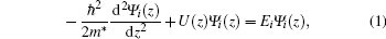
2. TheoryThe RTD structure as shown in Fig. 1 contains an active region composed of two barriers (AlxGa(1−x)N), a quantum well (GaN), and two undoped spacers: emitter and collector. In the framework of effective mass approximation, the Schrödinger equation in the growth axis direction for a confined electron is given by[23–25]
where

In the above equation, m* and VC(z) represent the effective mass of electron and the band offset, respectively. The band offset is given by the following expression:[26,27]

VH(
z) is the effective Hartree potential, which represents the electrostatic interaction of electrons with each other and with ionized impurities and
xrepresents the aluminum concentration.
VH(
z)can be found by solving the Poisson equation:
[23]

where
n(
z) represents the electronic density of the confined electrons,
ND(
z) is the total doping concentration, and
ε0εr is the dielectric constant. In Eq. (
3), the polarization-induced charge density is taken as
[28,29]
We solve the Schrödinger equation in the active region and the two contacts using the finite-difference method, by choosing one-dimensional uniform mesh a. The Schrödinger equation is then transformed into the following linear equations:


In the above equations, Δ = ħ2/2m*a2. L and R denote the left and right grid points.
In the hypothesis, the two region contacts are considered as perfect absorbers and the wave functions describing the propagation of free electrons are considered as plane wave functions. The incident waves on the right and left contacts take the following form:


By substituting Eqs. (7) and (8) into Eqs. (5) and (6), the Schrödinger equation describing the motion of electrons in the active region can be transformed to an N-dimensional matrix H, which can be written as follows:

where
ΣR,L = −
Δ exp(i
kLa) and
ΣR,R = −
Δ exp(i
kR a) represent the self-energies; they reflect the influences of the left and right contacts on the active region. In the (NEG) formalism, the retarded Green function
GR is considered as an important function because it contains the information about the distribution of the electronic states. After the eigenfunctions and eigenvalues are calculated from the Schrödinger equation, the retarded Green function can be calculated from the following expression:
[30]

where |
Ψi⟩ and
Ei denote the eigenfunctions and eigenvalues of the Hamiltonian
H, respectively. In the NEG formalism, the spectral function
A, which represents the local density of electrons, is related to the retarded Green function as follows:

where
Γ = i[
ΣR−
ΣR−1], and
GA =
GR* is called the advanced Green function. Thus, the local density of electrons
n(
z) is given by

where
fL(
E) and
fR(
E) are the Fermi functions of the left and right contacts, respectively. In the ballistic regime, the current density can be expressed as follows:
[23]
Equations (1)–(8) are solved self-consistently. The process is repeated until the difference between the two consecutive Hartree potentials becomes less than the desired tolerance  .
.
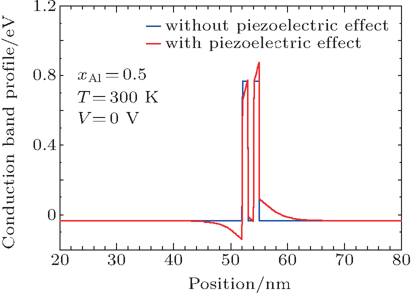
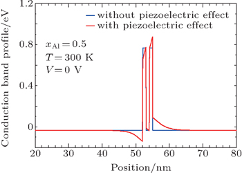
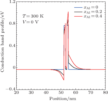
3. Results and discussionThe studied RTD consists of two barriers: AlxGa(1−x)N separated by GaN quantum well, and two undoped GaN layers acting as emitter and collector. The active region is sandwiched between two n-doped GaN layers (Fig. 1). In Fig. 2, the self-consistent result of the conduction band potential is presented. Without the piezoelectric effect, the potential profile is symmetric and no depletion region is formed; however, the piezoelectric and spontaneous polarizations produce surface charges at each GaN/AlGaN interface; these charges lead to the formation of a two-dimensional gas confined in the depletion region near the surface on the side of the emitter and collector. The polarization charges induced on the surfaces between GaN and AlGaN layers form a triangular quantum well. This effect can be very strong, and consequently affects the behaviors of the transmission coefficient T(E), the current density I(V), and the peak-to-valley ratio (PVR). To better understand this phenomenon, figure 3 shows the conduction band profile for three different values of aluminum concentration xAl, with the temperature fixed at 300 K. The obtained results show that the increase in the aluminum concentration increases the depth of the triangular quantum well formed between the left barrier and the emitter layer, and consequently the resonant energies are affected. This can be interpreted as follows: by increasing the aluminum concentration, the surface charges at each GaN/AlGaN interface also increase because of the variation in polarization discontinuity between the GaN and AlGaN layers. The discontinuities of the spontaneous and piezoelectric polarizations at the interfaces lead to the formation of the two-dimensional electron gas (2DEG) between the left barrier and the emitter; it means that the energy level positions in the active region should be dependent on the internal electric field because the potential well becomes a triangle. Thus, the triangular quantum well is pushed further from the conduction band edge in the contact layers; hence, the depletion region becomes larger, leading to a blue-shift behavior.
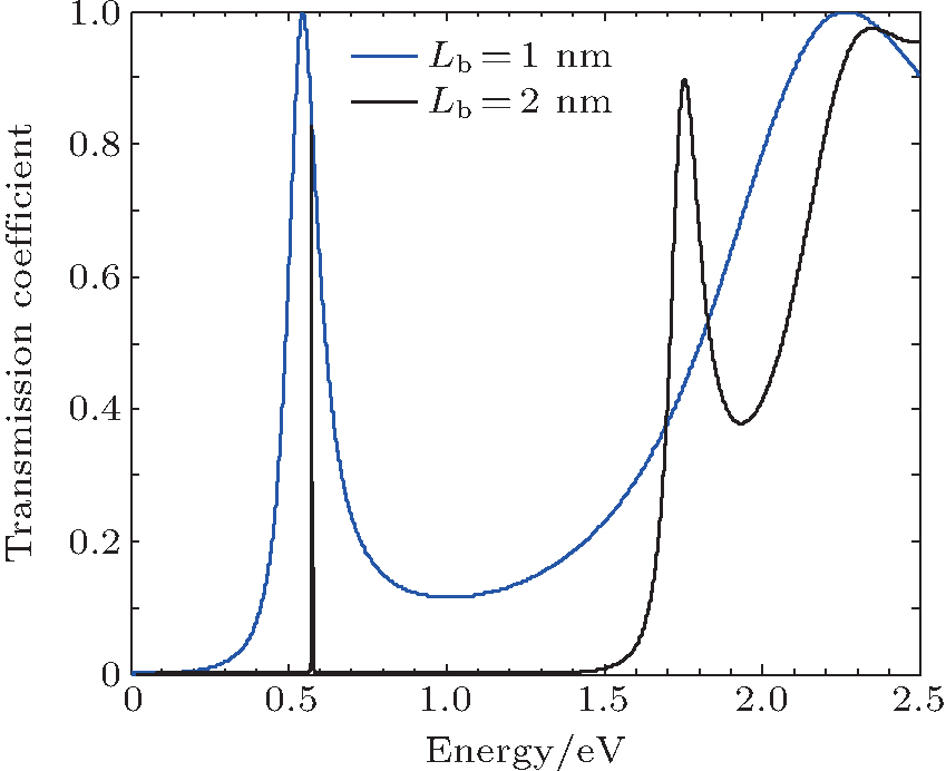
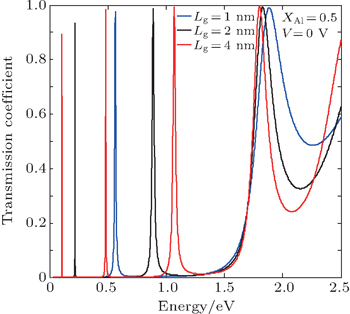
Figure 4 shows the transmission coefficients versus incident energy for different values of quantum well thickness Lg (nm). The active region considered in this case is composed of Lg (nm)-GaN quantum well bordered by two 1-nm-thick (i.e., Lb = 1nm) barriers of Al0.5Ga0.5N. The applied voltage is 0V and the temperature is fixed to be 300 K. It is clear that the transmission coefficient exhibits a series of resonant energetic levels. By increasing the quantum well width Lg, the number of oscillations increases and the peaks become sharper. In addition, we can conclude from this figure that the number of resonant states increases with the increase of the value of Lg (one resonant level for Lg = 1nm and three resonant levels for Lg = 2nm). Also, our study shows that the transmission coefficient contains a series of resonant peaks. The first series of resonant peaks is attributed to the resonant tunneling through the fundamental state in GaN quantum well; however, the second and third series of resonances are attributed to the quantum tunneling through the first and the second excited states respectively. The quantum tunneling phenomenon can be explained as follows. When the energy of the incident electron is equal to the resonant eigenenergy of the quantum well, the electron wave is trapped in the quantum well, reflecting back and forth between the barriers in such a phase as to produce constructive interference, and leaks out very slowly.[22]
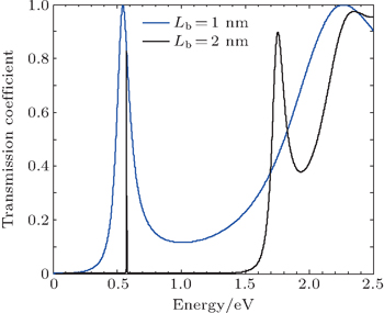
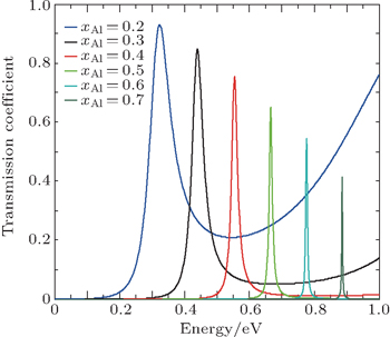
Figure 5 gives the transmission coefficients versus incident energy for different values of barrier Al0.5Ga0.5N thickness Lb (nm). To emphasize the effect of the barriers on the transmission behavior, three different values of barrier thickness Lb (nm) are simulated by fixing this time the GaN quantum well thickness at Lg = 1 nm. The transmission coefficient exhibits a series of resonances, but contrary to the previous case (Fig. 4), when the barrier thickness increases, the number and the energies of resonant levels are less pronounced. In Fig. 6, the variations of the transmission coefficient with incident electron energy for different values of aluminum compositions xAl are given. It is clear that with increasing the value of xAl, the resonant peaks are shifted toward higher energies and their transmission values decrease rapidly. In addition, it is clear that the peaks become deeper and sharper for high values of xAl. This can be explained by the fact that the increase in the aluminum composition xAl produces an important polarization discontinuity between the GaN and Al0.5Ga0.5N layers and therefore increases the surface charges at each interface. These charges produce an intense internal electric field, and consequently the triangular quantum well between the left barrier and the emitter layer is pushed further from the conduction band edge. Thus, the resonant energies are increased.
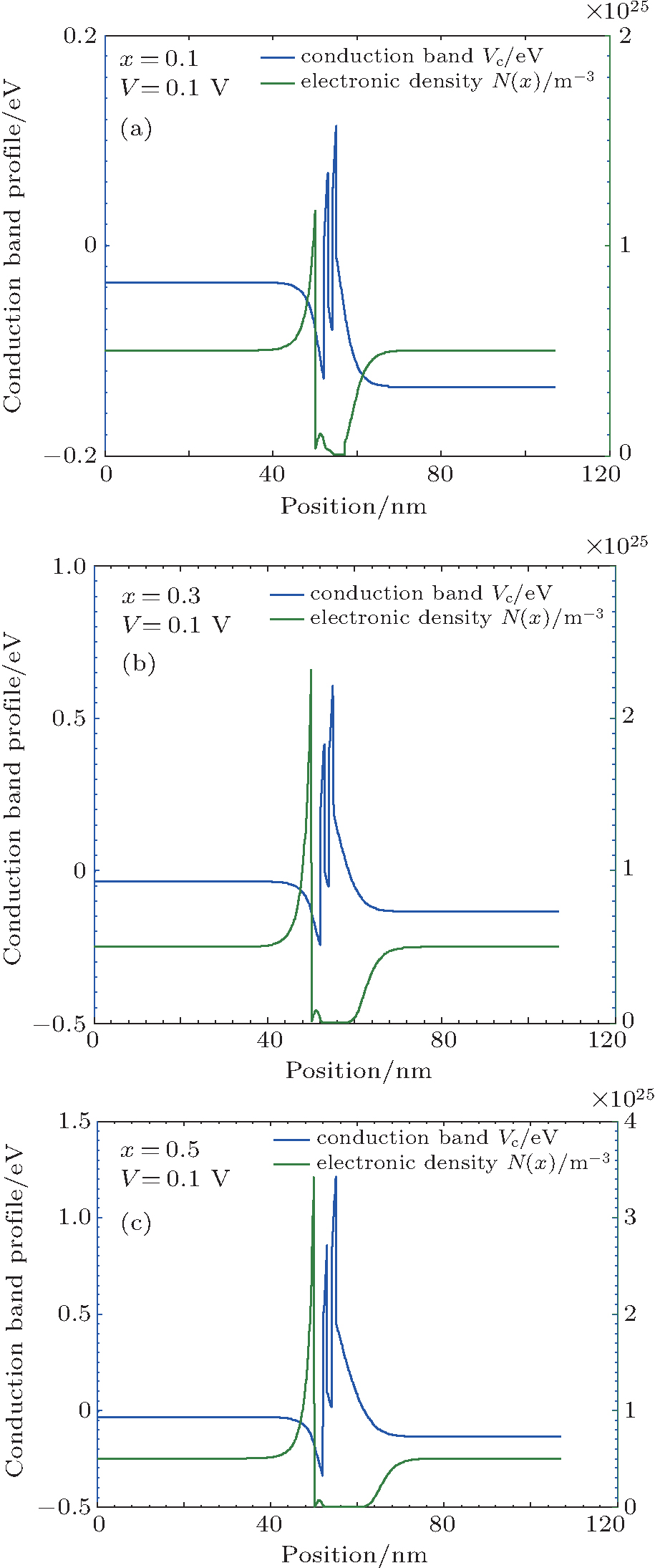
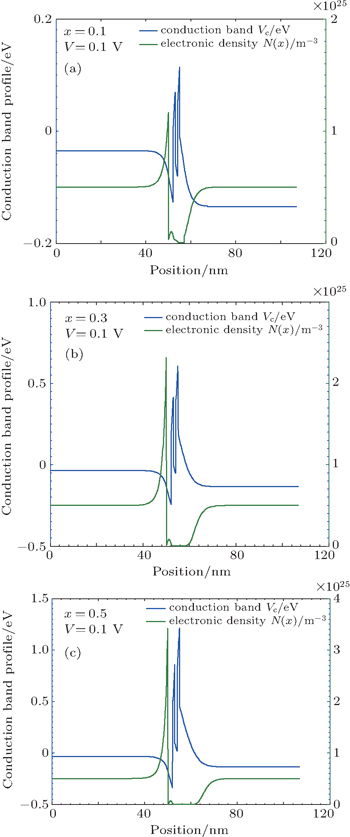
Figures 7(a)–7(c) represent the electronic densities in the RTD structure for three different aluminum concentrations xAl, respectively. The quantum well and the barrier width are fixed to be 1 nm and 1 nm, respectively. The significant result obtained from these figures is that the electronic density peaks sharply in the triangular quantum well region by increasing the aluminum concentration xAl (because of the higher values of the band offset Vc(z) and the effective mass of electron). However, for smaller aluminum concentration xAl, the electronic density is less sharp. The amplitude of the electronic density for lower aluminum concentration xAl (0.1 for example) is much lower than that for higher concentration. This phenomenon can be explained as follows: an increase in the aluminum concentration xAl enhances the conduction band offset Vc(z) between the GaN quantum well layer and the Al(1−x)GaxN barrier layers, thus increasing the barrier height and consequently enhancing the confinement of the electrons in the triangular quantum well. On the other hand, when the aluminum concentration xAl increases, the internal electric field produced by the spontaneous and piezoelectric polarizations becomes intense and distorts the symmetry of the potential profile. As a result, the energetic distance between the emitter and the left barrier becomes large, thereby increasing the depletion region and improving the confinement. Note that this strong confinement leads to a reduction in the width of the resonant level, thereby reducing the probability of the electron to tunnel the barriers. On the contrary, a reduced barrier height enhances the coupling between electrons and enlarges the resonant levels width but amplifies the tunneling probability.
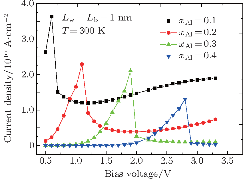
Figure 8 shows the variations of current density with applied bias voltage for different values of aluminum composition xAl. Apparently, the maximum of the current density decreases as the aluminum concentration increases. The effect of the NDR is clearly obtained for different applied bias voltages due to the difference in resonant energy level between cases. In addition, as shown in this figure, the peak current shifts progressively to higher voltages with the increase of aluminum concentration xAl. This behavior can be understood as follows: by increasing the aluminum concentration, the conduction band offset and the piezoelectric polarizations increase, leading to higher barriers and consequently a shift of the resonant current peaks toward higher voltages. In addition an increase of the aluminum concentration leads to a decrease of the current maximum. In addition an increase of the aluminum concentration leads to a decrease of the current maximum. This is explained by the fact that the bias voltage cancels the internal piezoelectric field introduced by the surface charges and consequently reduces the occupied electronic states. We conclude that the orientation of the external electric field has a great importance to adjust the output current by increasing or cancelling the internal piezoelectric field.
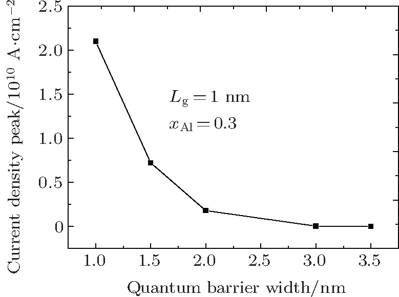
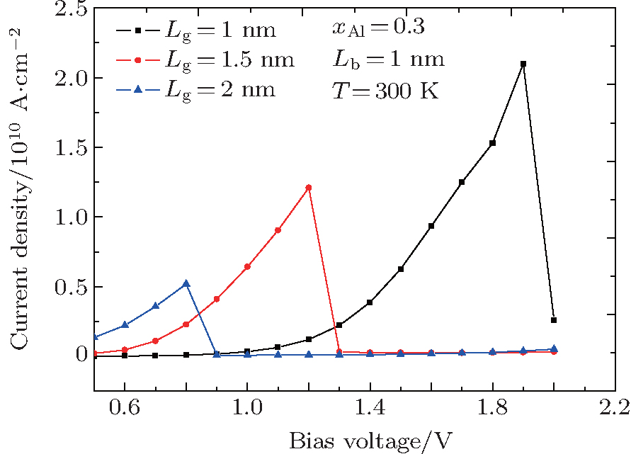
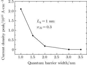
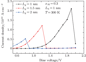
Figure 9 shows the dependence of the peak current on the barrier width. The well width is fixed to be 1 nm. It is clear from this figure that the current peak decreases with the increase of barrier width. The enlargement of the barrier thickness causes the peak current and the width of the resonant level energy to decrease. This phenomenon is obvious from the point of view of quantum mechanics since we take into consideration the fact that a thicker barrier reduces the tunneling probability of electrons across the barrier. The effects of the quantum well width on the current density for different bias voltages are given in Fig. 10. We remark that the peak of the current density decreases as the well width increases. At the same time, the PVR is reduced with width increasing. Figure 4 shows that the increase of quantum well width reduces the resonant energy levels and their half widths, which leads to the enhancement of the quantum confinement. Therefore, the transmission coefficients become sharper around the resonant energy levels. In that way, the current density is lower as the quantum well width becomes higher.
4. ConclusionsIn this paper, the effects of the quantum well width, the barrier thickness, and the aluminum concentration on the transmission coefficient and the current density in AlGaN/GaN RTD are investigated and explained using the nonequilibrium Green functions formalism (NEG). The results show how the quantum size and the aluminum concentration affect the current density and the potential profile. It has been shown that the spontaneous and piezoelectric polarizations introduce a strong asymmetry in the confining potential and create a two-dimensional gas in the depletion region, which has significant effects on the current density behavior. Also, from the results, it is revealed that the increase in the aluminum concentration reduces the transmission coefficient peak and leads to a blue-shift behavior. In addition, the barrier thickness strongly reduces the transmission coefficient. Our results also indicate that the PVR in the current density profile is reduced and the peak current is moved towards lower bias voltage by increasing the quantum well width for a given value of the barrier. The presented findings and the proposed device might be useful for various applications such as infrared photodetectors and ultrafast two-color devices.


 , Almansour S]