1. IntroductionGraphene is a promising material for ultrafast and ultra-broadband photodetection[1–8] because of its high carrier mobility[9] and broadband optical absorption.[10] Among reported graphene photodetectors, those with a self-powered photoelectric response[2,11–13] are particularly useful for device miniaturization and to save energy in integrated circuits. However, the reported self-powered photodetectors usually suffer from low photocurrent responsivity[11–13] because of the weak optical absorption of monolayer graphene[10] and ultrafast photogenerated carrier recombination in graphene[7,8] or a weak photothermoelectric effect.[14–16] Therefore, developing a self-powered graphene-based photodetector with high performance is highly desired, yet it remains a great challenge.
To realize an enhanced photoresponse under zero bias, two fundamental premises need to be satisfied simultaneously. One is to produce a large photovoltage between the electrodes, and the other is to enhance the non-equilibrium carrier density in graphene.[2,7,17] Regarding the former, a few studies on the photothermoelectric effect and very small photovoltaic responses of self-powered photodetectors have been reported.[1,2,16] In terms of the latter, various prototype devices involving integration of either quantum dots (QDs)[18] or an optical cavity[19] with graphene have already been demonstrated. However, both the QD and optical cavity-assisted routes are too complicated to meet the requirements of large-scale fabrication. Therefore, a simple device preparation procedure combined with a mature technique for advanced graphene production suitable for large-scale fabrication sensitive photodetectors is desirable. The potential of epitaxial graphene (EG) on silicon carbide (SiC) as a material for integrated electronic devices has been demonstrated.[20,21] If the advantages of graphene and SiC can be combined in a special device design consisting of a simple metal–graphene–metal structure with two-terminal electrodes exposed asymmetrically to ultraviolet (UV) light, a high-performance graphene-based UV photodetector without power supply may be obtained. Such a UV photodetector could find applications in both military and civilian fields.[22–24]
There are a few reports concerning the use of EG on SiC in photodetectors.[16,25,26] However, in the reported results, either the photon energy was deliberately smaller than the band gap of the SiC substrate to avoid influence from SiC[16] in a simple two-terminal graphene device, or a Schottky junction was used, where carriers in the circuit loop had to overcome the Schottky barrier between graphene and SiC, resulting in high power consumption.[26] Here, we demonstrate a graphene/SiC-based self-powered UV photodetector that exhibits a photocurrent responsivity of 7.4 mA/W with a response frequency of over megahertz under asymmetric 325-nm laser irradiation of one of the electrodes. The photogenerated carriers in SiC transfer to the irradiated electrode under the driving of interface field, so that a photovoltage of dozens of millivolts is built up between the electrodes with and without light irradiation. The built-in photovoltage responsivity is about four orders of magnitude higher than that of previously reported graphene-based photodetectors.[2,16] This graphene photovoltaic device or photodetector is compatible with modern semiconductor technology, making it attractive for use in UV imaging and graphene-based integrated circuits.
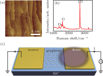
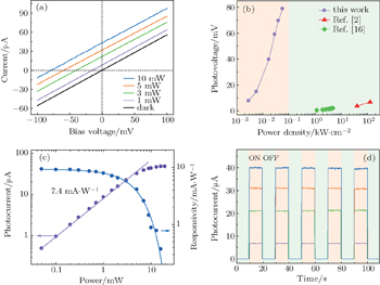
3. Results and discussionThe device structure and measurement electrical circuit are illustrated in Fig. 1(c). The current responses versus bias curves (I–V) for the device are shown in Fig. 2(a), while one of the electrodes was irradiated with UV light at different powers. With increasing irradiation intensity from 0 mW to 10 mW over a voltage range from −0.1 V to 0.1 V, the I–V curves shift upwards in parallel with each other, and they all exhibit linear behavior over the whole voltage range. In the dark (irradiation intensity is 0 mW), the I–V curve passes through the origin of the coordinates, indicating a good ohmic contact between the metal electrodes and EG. Here, the net photocurrent Iph = IUV − Idark is defined, which is the difference between the currents measured with and without light irradiation. The monotonic upward shift of the I–V curves with increasing UV light intensity indicates Iph is independent of applied voltage. The resistance of graphene deduced from the slope of the I–V curves was 1.78 kΩ, which is a reasonable value in the graphene device on SiC.[16] This relationship of photocurrent and applied voltage is similar to that observed in graphene PN junctions[11,12] and metal–graphene–metal devices under local light irradiation.[2,14,16]
Figure 2(a) indicates that a photovoltage ranging from several to dozens of millivolts is generated between the two electrodes, which can be directly derived from the interceptions on the x-axis; i.e., the zero-current voltages. A large photovoltage is extremely important for use as a self-powered photodetector. The dependence of the photovoltage on the UV light power density is plotted in Fig. 2(b) along with results reported for similar devices with two-terminal electrodes[2,16] for comparison. For clarity, the detailed data have also been summarized in the supplemental materials (Table SI, see Supplemental Materials). The photovoltage in this work is nearly four orders of magnitude higher than those observed previously[2,16] if normalized to power density. The large variation in photovoltage between our device and previous ones indicates that the photoresponse mechanism in our graphene/SiC UV photodetector is different from the reported photothermoelectric effect,[2,16] even though the devices all possess a simple two-terminal-electrode structure. The striking difference in the photovoltaic effect of this UV photodetector compared with that of the reported devices originates mostly from the contribution of the SiC substrate, which acts as a gain medium to provide photogenerated carriers to graphene and the electrode in the irradiated area. This situation is strongly supported by the results of a control experiment with a 632-nm laser, whose photon energy is lower than the band gap of SiC, irradiated on the electrode (Fig. S2, see Supplemental Materials). Therefore, in our device, both photovoltaic and photothermoelectric effects come into effect, but the photovoltage generated by the former is almost four orders of magnitude larger than that produced by the latter. A detailed discussion about the mechanism of photovoltage generation will be given later.
The dependences of photocurrent and responsivity of the device on laser power were extracted (Fig. 2(c)). The photocurrent stimulated by the UV laser increased linearly with incident power when the light intensity was relatively low, while it became saturated at higher power (> 10 mW). This is probably because of a screening effect of carrier transfer from SiC to the irradiated electrode similar to that noted in Ref. [17], where they consider a capacitor-like Coulomb repulsion effect is responsible for the saturated photocurrent at a higher incident power. A minimum response power of about 11 μW corresponding to a power density of 62 mW·cm−2 was deduced, which is three to four orders of magnitude lower than reported values.[2,16] In addition, the photocurrent responsivity Rph defined as Rph = IphP0,[5] where Iph and P0 are photocurrent and incident light power, is a constant 7.4 mA/W up to a power of 3 mW (power density: 17 W·cm−2). Then, Rph decreases with increasing light power. Here, Rph = 7.4 mA/W corresponds to a photovoltaic responsivity RV of about 13 V/W in a photovoltaic mode; it is equal to Rph multiplied by the resistance of the graphene device of 1.78 kΩ (Fig. 2(a)). The obtained Rph is about five to seven times higher than that reported for a conventional graphene–metal junction photodetector.[1,16]
The external quantum efficiency (EQE, ηe) for photon conversion into conducting electrons can be derived from the equation:[5]

where
h,
c, and
λ are the Planck constant, light speed in a vacuum, and incident light wavelength, respectively. Using
Rph = 7.4 mA/W, the maximum EQE of the device is about 2.8%. This is higher than the value reported for conventional graphene–metal junction photodetectors,
[1,2] but far lower than that of a QD-enhanced photodetector.
[18] The low EQE of the UV photoresponse is ascribed to the absorption of the 325-nm light by the metal electrode. About 99.6% of UV irradiation is absorbed and reflected by the Ti/Au (5 nm/60 nm) electrode and only 0.4% is transmitted to the SiC substrate (
Fig. S3, see Supplemental Materials), which is consistent with the results of a theoretical calculation using a finite-difference time-domain method.
[27] The theoretical result suggests that only about 0.5% of 325-nm UV light is transmitted to SiC, while 39.5% and 60% of the light are respectively reflected and absorbed by the Ti/Au (5 nm/60 nm) electrode. If the irradiated electrode is replaced by a mesh electrode, the built-in photovoltage will be increased and the photocurrent response and EQE of the device improved.
Besides the stable photocurrent response, the temporal photocurrent responses at zero bias voltage under on/off switching of UV light of different powers are depicted in Fig. 2(d), where the yellow and green time scales are respectively corresponding to the light on and off regimes. Sharp changes and repeatable responses of the photocurrent during the switching of UV light are observed. More detailed experiments about the response speed and stability of this UV photodetector were performed and are provided in the supplemental materials (Fig. S4, see Supplemental Materials). In transient photoresponse experiments, a continuous 325-nm laser was modulated by passing through a mechanical chopper with the highest frequency of about 110 kHz. The estimated response frequency of this graphene/SiC UV photodetector exceeds one megahertz (Fig. S4(a)). A stability test (Fig. S4(a)) demonstrated the photocurrent variation was less than 2% when the device was continuously irradiated for 8 h at 325 nm with a power density 30 W·cm−2. These results sufficiently demonstrate the fast response speed and high stability of the device, revealing that it is suitable for practical applications.
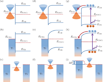
To understand the origins of the impressive photovoltage of this UV photodetector and the mechanism of its photoresponse, energy band diagrams of the heterojunctions between graphene, SiC, and metal Ti are depicted in Fig. 3. In this figure, EF(G), EF(SiC), and EF(Ti) are the Fermi levels of graphene, SiC, and metal Ti, respectively, while ECB (EVB) represents the conduction (valence) band energy of SiC. The band gap and electron affinity energy of semi-insulating 6H–SiC are 3.03 eV and 3.45 eV,[28] respectively. The graphene is p-type doped and has a Dirac point of about 4.5 eV relative to the vacuum level,[29] and the work function of Ti is about 4.3 eV. Therefore, energy band edge configurations before equilibration appear as shown in Figs. 3(a)–3(c). After the device constituents are contacted with each other, the band edge configurations illustrated in Figs. 3(d)–3(f) are formed. Under UV irradiation, the photogenerated carriers in SiC are transferred to graphene and Ti, increasing the Fermi level of the irradiated electrode to a stable value of ΔE relative to the electrode without UV illumination, as shown in Fig. 3(i). Therefore, a photovoltage ΔE/e is generated between the two electrodes. The built-in voltage drives the electrons in graphene to move against the electric field, leading to a short-circuit photocurrent response even without any external power supply (Fig. 2(d)). The direction of the short-circuit photocurrent is shown in Fig. 1(c). Within this fundamental physical framework, the prominent performance of the UV photodetector can be ascribed to two effects. The first is that the photogenerated carriers produced in SiC are quickly transferred to the electrodes or graphene driven by the interface electric field between them. The second is the generation of the photovoltage between the electrodes with and without UV irradiation, which results in a short-circuit photocurrent. Here, SiC plays roles as both a supporting substrate and a photoresponse medium providing photogenerated carriers to the irradiated electrode, while graphene acts as a sensitive response medium for photogenerated carrier transfer in a confined manner because of its few monolayers structure. It is the few layers thick graphene that renders the latter effect. To support these inferences and understand the role of graphene, control experiments that involved connecting the electrodes with the same metals (Fig. S5, see Supplemental Materials) and removing the graphene (Fig. S6, see Supplemental Materials) were performed. The results demonstrate that graphene is not only an excellent carrier-conducting medium but also a carrier confinement medium because of its atomic-layer thickness, which allows photogenerated carriers to partially accumulate at the irradiated electrode. This evidence strongly indicates that our graphene/SiC photodetector is clearly distinguished from the devices that operate through the well-known photothermoelectric effect realized by light irradiation of a local area of a graphene channel,[11,12] local chemical doping,[13] electrostatic splitting gates,[30] or electrodes with different work functions on graphene.[2,16]


 , Lu Wei1, Zhang Yong-Hui2, Shi Zhe3, Jia Yu-Ping1, Li Zhi-Lin1, Yang Jun-Wei1, Chen Hong-Xiang1, Mei Zeng-Xia2, Chen Xiao-Long1, ‡,