1. IntroductionGermanium (Ge) has the potential to be engineered to become a direct band gap material for an on-chip integrated light source due to the fact that its direct-to-indirect band separation is only 140 meV at room temperature.[1–3] Until now, three key methods to tune the Ge band structure to a direct or quasi-direct band gap material are still under research: the first one is heavily n-type doping Ge,[4,5] the second one is biaxial tensile strained Ge,[6,7] and the last one is germanium-tin (Ge1 − xSnx) alloy.[8–10] With heavily n-type doping in Ge, the indirect L valleys are filled by the extrinsic electrons thermally activated from the n-type donors, and there is a higher possibility for the excess electrons to thermally occupy the Γ valley of the conduction band, contributing to the direct gap light emission.[11] Therefore, doping in Ge, especially n-type doping, will play a significant role in improving the efficient radiative recombination of Ge at the Γ point.
To date, there have been many schemes to realize the heavily n-type doping Ge and improve the light emission efficiency. As is well known, ion implantation is an efficient technique to increase doping concentration in Ge. However, interstitial point defects which can damage the Ge structure by adding extra optical losses are also created through implantation.[12] The in-situ doping technology, which is natural to dope the Ge film during the epitaxy, is another way to achieve heavily n-type doping Ge without any implantation-related damage compared with the implanted Ge films. It avoids deep in-diffusions of dopants and provides fairly shallow junctions while offering high electrically activated concentrations at low processing temperatures.[13–16] However, many challenges, including difficulty in finding the suitable n-type dopant with high solubility and low diffusivity, and difficulty in preparing the heavily n-type doping Ge with high crystal quality, also need to be solved to achieve heavily n-type doping Ge by the in-situ doping technology.
In this paper, the detailed properties of n-Ge epilayer on Si substrate, prepared with in-situ doping technology in UHVCVD, are presented including the optimal growth temperature, depth profiles of phosphorus concentration, surface morphologies, strain status, and photoluminescence.
2. Experimental methodsSeveral phosphorus in-situ doped Ge epilayers on Si substrate are prepared in a cold-wall UHVCVD, with a base pressure of 5 × 10⁻⁸ Pa. A reflection high-energy electron diffraction (RHEED) apparatus is equipped to monitor in situ and in real time the Ge growth mode in the growth chamber. Pure Si2H6 and GeH4 are used as the sources of Si and Ge, respectively. Phosphine (PH3) diluted at 0.5% in H2 is used for n-type doping.
The silicon substrates are treated with standard RCA (Radio Corporation of American) cleaning, and then they are baked in the growth chamber to de-oxidized at 850 °C for 30 min. After that, a 300-nm-thick Si buffer layer is grown at 750 °C, followed by a 520-nm Ge virtue substrate (VS) grown at 600 °C with a low-temperature self-patterned Ge coalescence island template. Then about 400-nm phosphorus layers doped Ge with various doping concentrations are grown at 450 °C, 500 °C, and 630 °C for 2 hours by controlling the ratio of PH3 gas flow to GeH4 gas flow in the growth chamber. More details of the growth conditions can be found elsewhere.[17,18]
The doping concentrations of the samples are estimated by the four-point probe method and confirmed by secondary ion mass spectrometry (SIMS). The surface morphologies of the samples are analyzed by atomic force microscopy (AFM) in a tapping mode. The double crystal x-ray diffraction (XRD) is employed to evaluate the strain status and crystal quality of the samples. The photoluminescence (PL) is measured at room temperature using an Ar+ laser emitting at 488 nm to characterize the optical properties of the samples.
3. Results and discussionAs is well known, in-situ doping is a complicated process that may be affected by many parameters such as the gas flow, the growth temperature and the base pressure in the growth chamber. In order to optimize the growth of n-Ge, the doping concentrations in n-Ge epilayers grown with various PH3-to-GeH4 gas flow ratios at growth temperatures of 450 °C, 500 °C, and 630 °C are studied, and the results are shown in Fig. 1. Here, the doping concentrations are the average active doping concentrations which are estimated from the sheet resistance and the film thickness measured by a selective etch approach. In Fig. 1, it can be seen that the doping concentrations increase slightly with the PH3-to-GeH4 gas flow ratio increasing at a given temperature, which indicates that more P atoms will be dissolved into Ge in the growth process with the increase of PH3. Besides, at a given PH3/GeH4 flow ratio, the growth temperature of 500 °C may be an optimal temperature to obtain a higher doping concentration for the n-Ge growth in our equipment. It may be due to the fact that phosphorus concentration is mainly limited by the dissociation of adsorbed PH3 molecules on the surface at low temperature, and a surface segregation or out diffusion of P atoms may become dominant at high temperature.
It is worthy to be noted that the effect of growth temperature on n-Ge epilayers can be different in different growth systems. The doping concentration decreases as temperature increases from 3.6 × 1020 cm−3 at 400 °C down to 1019 cm−3 at 750 °C in reduced pressure chemical vapor deposition (RPCVD), which is reported in Ref. [14]. Also, in the hot-wall UHVCVD, the doping levels in Ge films decrease at both high temperatures and low temperatures as reported in Refs. [5] and [19], and the growth temperature of ∼650 °C is optimal for a maximal doping concentration of 1 × 1019 cm−3. However, only ∼1018 cm−3 n-type doping concentration at a growth temperature of ∼500 °C has been achieved by in-situ doping technology in our cold-wall UHVCVD system. It may be due to the cold-wall system, which means that additional cooling applied to the chamber wall can affect the desired pressure during the growth.
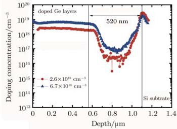
The typical SIMS depth profiles of the n-Ge epilayers on Si substrate with doping concentration of 2.6 × 1018 cm−3 and 6.7 × 1018 cm−3 are shown in Fig. 2. It is shown that the depth profiles of phosphorus concentration are box-shaped for the samples. However, phosphorus diffuses into the intrinsic Ge layer with slight decreasing of dopant concentration during the growth of the n-Ge epilayer. This is because the point defects in the Ge epilayer accelerate the diffusion of phosphorus into the undoped Ge layer. The arising phosphorus concentration in the Ge VS may be due to SiH arising from hydrogen adsorption at the Ge/Si interface or the phosphorus accumulation in the low temperature undoped Ge buffer layer with high dislocation density as reported in Refs. [17], [20], and [21]. It should be noted that the doping concentrations measured by SIMS are a little higher than the average active doping concentration, which indicates that the phosphorus in the n-Ge epilayers on Si substrate are not activated at all.
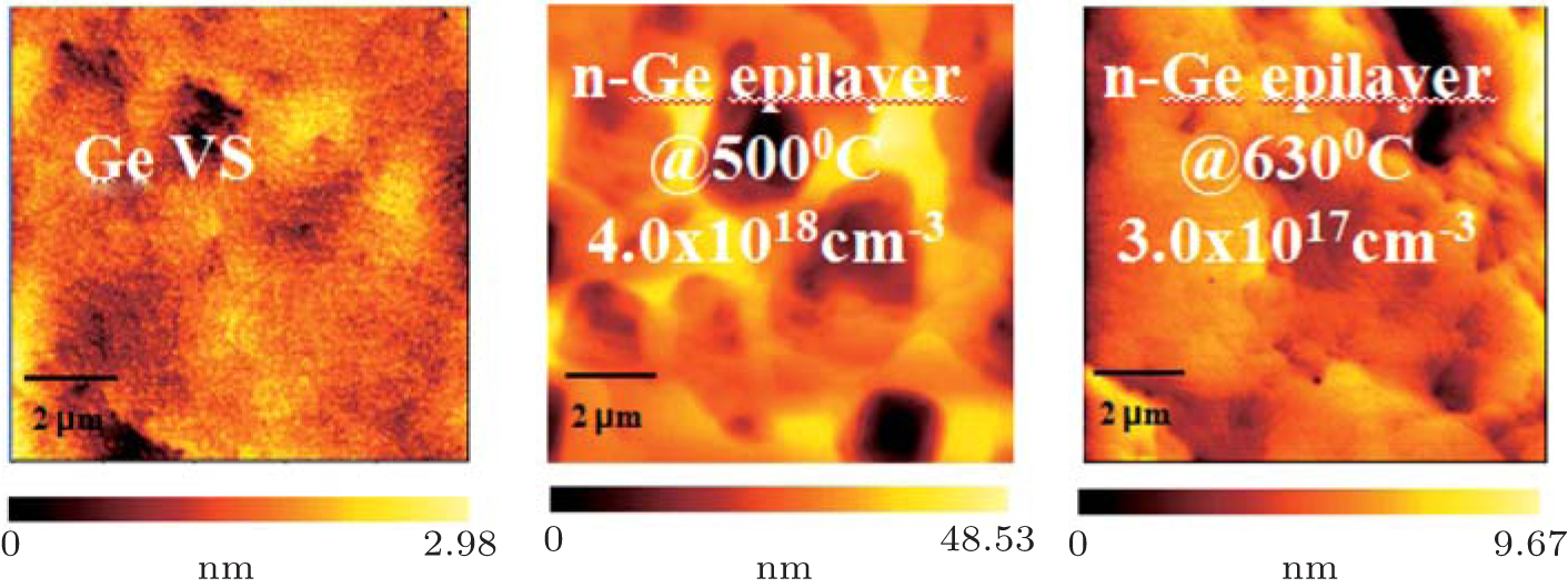
The variations in roughness with growth temperature are shown in Fig. 3 typically. For the Ge VS grown on Si, a root mean square (RMS) surface roughness is 0.45 nm, which is smooth enough for growing the n-Ge epilayer. However, the surface morphologies of n-Ge epilayers below 500-°C growth temperature are rough with an RMS roughness value of about 7 nm. Typically shown in Fig. 3 is an RMS roughness value of 6.5 nm with a doping concentration of 4.0 × 1018 cm−3 at 500-°C growth temperature. The enhancement of RMS roughness at low temperature (below 500 °C in our system) may be a result of the surface poisoning effect that the available epitaxial growth sites on the growth surface are occupied by other molecules such as PH, which are also observed for phosphorus in situ doping in Si.[22] When the growth temperature increases to 630 °C, the RMS roughness decreases to 1.5 nm with the doping concentration decreasing to ∼1017 cm13. This behavior indicates that the surface chemical reactions are generally thermally activated and the phosphorus atoms adsorbed in the Ge surface tend to be desorbed from the surface at high temperature, leading to lowering the dopant concentration.
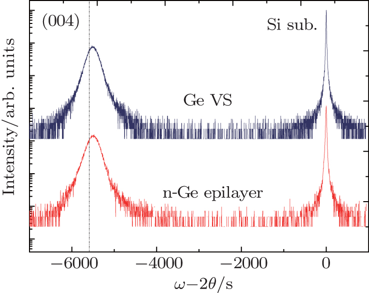
Double crystal x-ray diffraction (XRD) is performed on the n-Ge epilayer in order to examine the crystal quality and strain status. The typical ω–2θ symmetric (0 0 4) XRD scan of the n-Ge epilayer and Ge VS are shown in Fig. 4. Two peaks originating from Si substrate and Ge epilayer are clearly observed. The Ge diffraction peaks of the two typical samples are symmetric and sharp, indicating the good quality of the epitaxial n-Ge film and Ge VS. On the other hand, compared with the bulk Ge (straight dotted line showed in Fig. 4), the smaller peak distance between Ge and Si substrate indicates that the epitaxial n-Ge layers and Ge VS are under tensile strain. From the peak positions, both in-plane tensile strains of the samples are evaluated to be 0.12%, according to Bragg’s law with λ = 0.15406 nm for Cu K1 radiation. The strain in the sample mainly arises from the differences in the thermal expansion coefficients between Ge and Si. The XRD measurements confirm that the tensile strains of all the samples are about 0.12%, and the doping does not contribute to releasing or increasing the strain in the growth process.
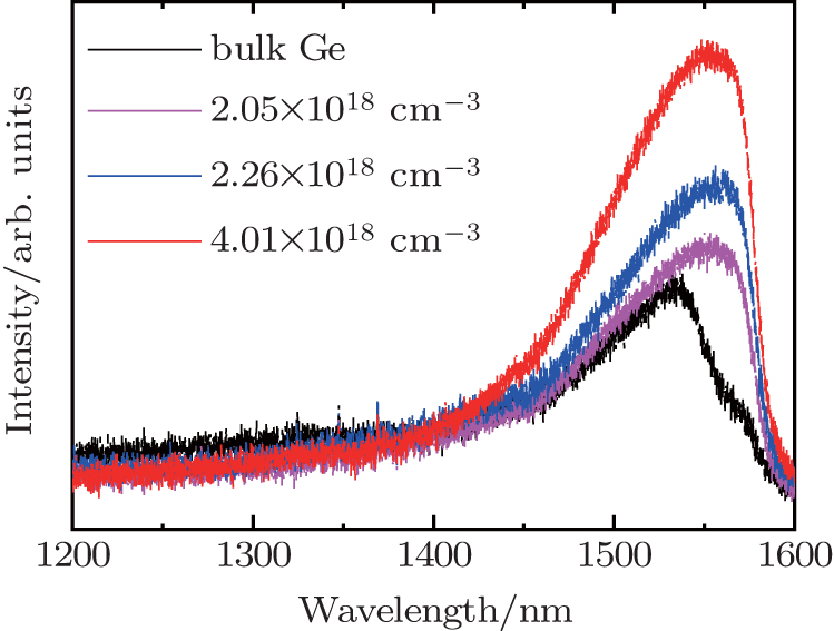
Room temperature photoluminescence of the n-Ge epilayers are measured with an InGaAs detector array cooled by liquid nitrogen. As shown in Fig. 5, the result of direct band transition energy in bulk Ge at room temperature is located at 0.816 eV (corresponding to 1520 nm), which is 16 meV higher than the direct band gap of bulk Ge 0.80 eV (corresponding to 1550 nm), due to the distribution of the carriers following the Boltzmann distribution (about 13 meV higher than the direct band gap at room temperature). Also, the photoluminescence peak of direct band transition energy shifts to lower energy by about 15 meV for the n-Ge epilayer compared with that of bulk Ge, which indicates that a shift of the band gap will be introduced in the n-Ge epilayer.
A shift of the band gap in the n-Ge epilayer maybe lies in two aspects: band gap narrowing effect due to doping in the n-Ge film[23] and tensile strain in n-Ge epilayer.[6] For the former one, a significant band gap narrowing effect will occur in the degenerately n-doped Ge film, that is, doping level will be higher than 1 × 1019 cm−3.[21] To our samples, the quasi-Fermi levels are under the L-band, which indicates that a red-shift in the photoluminescence spectrum of the film does not result from the band gap narrowing. For the latter, the XRD curve indicates that the tensile strain in the n-Ge epilayer is about 0.12%, corresponding to the reduction of 17.5 meV in the direct band gap of Ge, which is matched with the red shift of 15 meV in the PL curve of n-Ge epilayer. It indicates that the red shift of photoluminescence comes from the tensile strain in the n-Ge epilayer.
On the other hand, PL intensity of the sample is enhanced with n-type doping concentration increasing as shown in Fig. 5. The spontaneous emission spectra of the direct band transition in Ge with various doping concentrations at room temperature are simulated to analyze the observed enhancement of the PL intensity, by taking into account n-doping in Ge as shown in the Fig. 6.
The spontaneous emission spectrum for direct transition Rsp can be expressed as

Here, τr is the radiative lifetime (10−10 s);[24] hv is the direct band absorption coefficient of Ge;

with
A being constant,
EgΓ the direct band gap of Ge;
fc(
hv) and
fv(
hv) are the conduction and valence Fermi–Dirac distributions at room temperature. In the simulation, we assume that all dopants are activated and only 0.12% tensile strain in the Ge epilayer is considered. The calculated emission spectra are shown in Fig.
6. It is found that the spontaneous emission rates increase with the doping concentration increasing, which is consistent with the experimentally observed increase of the photoluminescence signal.
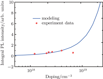
The enhancement of integral PL intensities (from modeling and experimentally measuring data) with the increase of the doping concentration is shown in Fig. 7. In the calculation, the PL spectrum amplitudes are normalized to unity for comparison. It is shown that the direct gap integral PL intensity is proportional to the electron concentration in the Γ valley and the hole concentration at quasi-equilibrium state under excitation.
4. ConclusionsIn this study, we exhibit the properties of n-Ge epilayer on Si substrate with in-situ doping technology in UHVCVD. The growth temperature of ∼500 °C seems to be an optimum temperature for growing the n-Ge epilayer in our system with a phosphorus concentration of ∼1018 cm−3. SIMS depth profiles of the n-Ge epilayer indicate that the distribution of dopant is box-like. XRD curves show that the tensile strain of the n-Ge epilayer is the same as that of Ge VS, which indicates that the doping does not contribute to releasing or increasing the strain in the growth of n-Ge epilayers. The tensile strain dominantly contributes to the red shift of the PL in the n-Ge epilayers. The simulation of spontaneous emission spectrum of the direct band transition in Ge shows that the PL intensity increases with the increase of doping concentration in the n-Ge epilayer, which is consistent with the experimental data. The studies will enable efficient application of Ge-based devices.


 , Li Cheng2, Chen Cheng-Zhao3, Wang Chen2, Xie Wen-Ming1, Lin Shu-Yi1, Shao Ming1, Nie Ming-Xing1, Chen Cai-Yun1]