Optical control of light propagation in photonic crystal based on electromagnetically induced transparency
Wang Dan1, 2, Wu Jin-Ze1, 2, Zhang Jun-Xiang1, 2, †,
The State Key Laboratory of Quantum Optics and Quantum Optics Devices, Institute of Opto-Electronics, Shanxi University, Taiyuan 030006, China
Collaborative Innovation Center of Extreme Optics, Shanxi University, Taiyuan 030006, China


† Corresponding author. E-mail: junxiang@sxu.edu.cn

Project supported by the National Natural Science Foundation of China (Grant No. 11574188) and the Project for Excellent Research Team of the National Natural Science Foundation of China (Grant No. 61121064).

Abstract
Abstract

A kind of photonic crystal structure with modulation of the refractive index is investigated both experimentally and theoretically for exploiting electromagnetically induced transparency (EIT). The combination of EIT with periodically modulated refractive index medium gives rise to high efficiency reflection as well as forbidden transmission in a three-level atomic system coupled by standing wave. We show an accurate theoretical simulation via transfer-matrix theory, automatically accounting for multilayer reflections, thus fully demonstrate the existence of photonic crystal structure in atomic vapor.

1. Introduction

Electromagnetically induced transparency[1,2] (EIT) is a fascinating quantum coherence phenomenon to suppress resonant absorption[3] and slow light pulse,[4] manipulate atomic entanglement,[5] and realize high efficiency quantum memory.[6,7] It has been successfully integrated on a semiconductor chips,[8] promoting the development of quantum optical device. Recently, EIT shows the wide applications in the field of cavity optomechanics,[9] optical lattice for cold atoms,[10] and hybrid atom-molecular system.[11,12] Photonic crystal structure[1316] with periodically varying refractive index is capable of controlling the flow of light wave. The main feature is to open photonic band gaps (PBGs) resulting from Bragg scattering.

The combination of EIT and photonic crystal is an attractive research for quantum communication network. EIT-based photonic crystal structure can be constructed in a three-level atomic system driven by a standing wave, which results in spatially modulated absorption and refractive index.[17] This photonic crystal structure generates a reflected field, which is explained as either electromagnetically induced grating (EIG)[1820] or four-wave mixing (FWM) process.[21,22] At the same time of reflection, electromagnetically induced absorption (EIA)[23] happened to the probe field in thermal vapor. Therefore, much attention has been paid to the applications in all-optical routing,[24] optical controllable Bragg mirror,[25] and optical diode.[26] Bae et al. and Andy et al. observed reflection signals with efficiencies of 11.5%[20] and 7%,[24] respectively, accompanying a decrease in transmittance of the probe field[19,20,24] due to EIG reflections and spatial interference effects from the modulated absorption in rubidium atoms. For the application in high performance quantum optical device, we should improve the reflection efficiency to a higher level as well as achieve strong absorption. Here, we experimentally obtain 35% reflection and simultaneously achieve the complete opaque to the probe field in a spatially modulated photonic crystal grating with cesium vapor.

In these previous studies, diffraction/reflection signals were obtained by solving the wave equation of the probe field with the consideration of spatial modulation of coupling field.[18] On the other side, the explanation of FWM[21,22] focused on the nonlinear susceptibility exploiting perturbation theory without regard to the spatial modulation. In the present paper, by combing the periodic modulation and EIT, we show good agreement between numerical simulation and experimental observation with using the transfer-matrix theory,[27,28] which is proved to be the most effective method to study the light propagation in periodically modulated dielectric. The consistence fully demonstrates the existence of periodic modulation thereby helpfully understanding the physics behind multilayer reflections in photonic crystal structure.

2. Experiment

We perform the experiment in a three-level system with one excited level |a〉 (62P1/2,F′ = 4), and two ground levels |b〉 (62S1/2,F = 4) and |c〉 (62S1/2,F = 3) of the 133Cs D1 line, see Fig. 1(a). The resonant transition frequencies of |a〉 ↔ |b〉 and |a〉 ↔ |c〉 are denoted as ωab and ωac, respectively. Spontaneous decay rate of the excited level is Γ = 2π × 4.6 MHz. Two counter-propagating horizontally linearly polarized coupling fields with equal frequency ωc = ωac propagate along the x direction. A vertically linearly polarized probe field ωp is frequency scanned in the vicinity of |a〉 ↔ |b〉 with detuning Δp = ωpωab and enters into the vapor cell at an angle of θ = 0.14° with respect to the coupling field. In experiment, we control the atom temperature at T = 60 °C. The powers of the counter-propagating coupling fields are both 20 mW with e−2 full width of 0.64 mm, and the power of the probe field is 50 μW with e−2 full width of 0.59 mm. The probe intensity is detected by PD1, and the reflective field (blue dashed line) is collected by PD2 in the reverse direction.

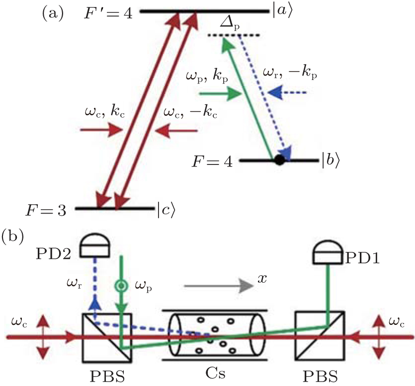
Fig. 1. (a) Λ-type three-level system driven by standing wave (SW) coupling field. (b) Experimental setup. PBS: polarizing beam splitters, PD: photo detector.

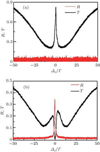
If the backward coupling field is blocked, this atom-field interaction exhibits typical EIT as shown in Fig. 2(a). There is no reflection signal to be detected by PD2, at the same time, the probe field propagates with transmission T = 80% at resonant frequency (T = Pout/Pin, Pout and Pin are the powers of the output and input probe fields). When the backward coupling field is switched on, an SW is formed with intensity modulation at half wavelength. Then, the probe absorption is periodically modulated as a grating. This grating structure results in the reflection signal of probe field with efficiency R = 35% (R = Pr/Pin, Pr is the power of the reflected field), see the red curve in Fig. 2(b). The generation of reflection signal can be explained as either FWM[21,22] or Bragg scattering[1820,24] originating from the periodicity of refractive index. We will focus on the latter explanation in the following. The accompanying transmission at one- and two-photon resonance Δp = 0 is transformed from EIT into forbidden transmission, see the black curve in Fig. 2(b). This forbidden transmission is the result of velocity selective effect. For thermal atoms moving with nonzero velocity along the x direction, the frequencies of the counter-propagating coupling fields are different from each other due to Doppler Effect. Therefore, the on-resonance enhanced absorption is attributed to the interaction with slow atoms, and two transparency windows around the resonant point are EIT contributed by two groups of atoms with opposite velocities. In a word, high-efficiency reflection as well as completely opacity is consistent with the effect of photonic band gap, and it is promising to be applied as a quantum optical device.

Fig. 2. The probe reflection (red curve) and transmission (black curve) spectra. (a) Typical EIT when the backward coupling field is absent. (b) The atomic system is coupled by SW.
3. Theoretical calculation

SW coupling field varies the absorption of probe field along the x direction with a periodicity of a = λc/2. Then, the periodical modulation of absorption gives rise to a similar modulation of refractive index limited by Kramers-Kronig relations[29] as shown in Fig. 3. The probe field “sees” the atomic vapor like a one-dimensional (1D) array of thin atomic slabs with periodicity a.

3.1. Periodic modulation of the refractive index

Considering the optical transition of |a〉 ↔ |b〉 driven by the weak probe field, off-diagonal density matrix element ρab is represented as a Fourier series in this periodical modulated dielectric

which is the superposition of infinite spatial harmonics. In Eq. (1), kp and kc are the vacuum wavenumbers of the probe and coupling fields respectively. The Rabi frequencies of the probe, forward and backward coupling fields are denoted as Ωp, Ωc1, and Ωc2, respectively. Fourier coefficients are solved by the method of continued fractions.[21,22]

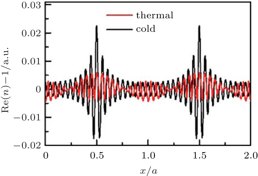
Fig. 3. Periodic refractive index pattern. Red curve (multiplied by a factor of 100) is for the thermal atoms with N0 = 1016 m−3, black curve is for the ultracold atoms with N0 = 1018 m−3. Other parameters are Ωc1 = Ωc2 = 5Γ, Δp = 0.05Γ, and λc = 894.576 nm.

For an atom moving with velocity v along the x direction, the frequencies of the probe, forward and backward coupling fields are Doppler shifted by kpv, kcv, and −kcv, respectively. Consequently, the two counter-propagating coupling fields have a frequency difference 2kcv. The optical responses for all atoms with Maxwell velocity distribution are calculated by integrating Eq. (1) with

where is the most probable velocity of atoms at a given temperature T, ma is the atomic mass, and kB is the Boltzmann constant λ0 = 894.6 nm and γab = 0.5Γ are the resonant wavelength and decoherence rate of transition |a〉 ↔ |b〉, respectively and N0 is the atomic number density. Thus, complex refractive index .

It can have a good accuracy to sum the spatial harmonics from n = −20 to 20 in Eq. (1). Consequently, Re[n(x)] − 1 exhibits a spatial modulated wave packet with periodicity a as shown in Fig. 3. Compared with ultracold atoms, blurry spatial modulation of refractive index is shown in thermal atoms because of Doppler shift and smaller atomic density.

3.2. Probe reflection and transmission

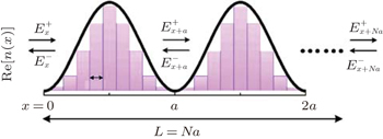
Transfer matrix relates forward- and backward-going waves on both sides of an arbitrary optical element.[27] In order to describe the probe propagation through multilayer dielectric, the field amplitude at arbitrary position x is divided into both forward- and backward-going parts as shown in Fig. 4, and regarded as the two elements of a two-dimensional (2D) column vector.

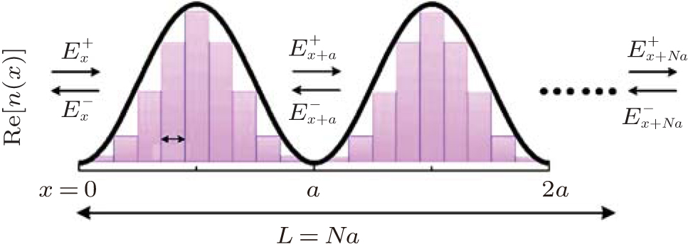
Fig. 4. Illustration of transfer-matrix method in a periodical modulated 1D atomic array.

As shown in Fig. 3, the photonic crystal structure is not an array of homogeneous thin atom layers but an array of inhomogeneous thin atom layers with a function of n(Δp,x) in each period. To obtain more accurate numerical simulation, we divide single period into l small slices with each slice occupying an identical thickness of a/l, sufficiently smaller than a. The more slices is divided, the more accurate simulation will be obtained, see Fig. 4. The probe field amplitude experiencing a single period is expressed by

where E+ and E are the forward and backward-going parts at arbitrary position, respectively, M is the primitive cell transfer matrix, and mj is the transfer matrix of the j-th slice in one cell[27] with

with det, mj = 1 and det M = 1. For simplicity, we denote n[Δp,x + (j − 1)a/l] as n.

The grating period is a = λc/2 ≈ 447 nm, therefore, 75-mm-long atomic vapor can be regarded as the stack of an abundance of but finite periods in experiment, whose length is L = Na (N ≫ 1 is the number of periods). The probe amplitude at the exit of the cell is expressed by

where MN = MN = uN−1 (α) MuN−2 (α) I, with I being a 2 × 2 identity matrix,

and α = TrM/2.[27]

In addition, transfer matrix MN holds the expression of
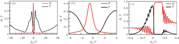
where RN and TN are the amplitude reflectivity and transmittivity of the incident probe field respectively. Finally, one obtains

where M12 and M22 are the elements of M. Then, we can directly study the probe reflection R = | RN |2 and transmission T = | TN |2 spectra.

3.3. Numerical simulation

Figure 5(a) shows a very accurate numerical simulation of probe reflection and transmission spectra with taking into account the periodic modulation of refractive index. The consistence between theory and experiment demonstrates that the efficient on-resonance Bragg reflection signal and strong absorption are both induced by photonic crystal structure based on EIT. Near-resonant expanded view for Fig. 5(a), which is shown in Fig. 5(b), shows that the sign of photonic stop band gap occurs in thermal vapor. The location of this PBG is limited by Bragg condition λ0 = n(Δp)λc cos θ. Therefore, the gap position is optically tunable by controlling the wavelength of coupling field and angle between coupling and probe fields. Referring to result shown in Fig. 3, large spatial modulation of refractive index in ultracold atoms is probable to open a perfect band gap. Therefore, we plot the probe reflection and transmission in Fig. 5(c). Perfect PBG occurs in the frequency region of Δp ∈ [0,0.16Γ] with nearly 100% reflection and zero transmission.

Fig. 5. Theoretical simulations of probe reflection (red curve) and transmission spectra (black curve). Panels (a) and (b) are for Doppler-broaden thermal atoms with u = 250 m/s, panel (b) is for the near-resonant expanded view in panel (a), the other parameters are the same as those in Fig. 3. Panel (c) is for the ultracold atoms driven by non-perfect SW with Ωc2/Ωc1 = 0.8. In numerical calculation, a single period is divided into l = 50 slices and the number of periods is set to be N = 1.6 × 10⁵.
4. Conclusion and perspectives

In this work, we experimentally investigate a kind of photonic crystal structure in three-level cesium vapor driven by standing wave coupling field. A similar effect of frequency stop band, on-resonance high-efficiency Bragg reflection signal and forbidden transmission are obtained. Transfer-matrix method is used to give a very good numerical simulation with taking into account the characteristic of periodic refractive index modulation. It is proved that photonic crystal structure really exists in this coupled atom-field system due to the consistence between experimental and theoretical results. Furthermore, perfect PBG is predicted in ultracold atoms, providing potential applications in optical communication network and promise to be integrated on chip.

Reference
1Harris S E 1997 Phys. Today 50 36
2Wang MBai J HPei L YLu X GGao Y LWang R QWu L AYang S PPang Z GFu P MZuo Z C 2015 Acta Phys. Sin 64 0154208 (in Chinese)
3Xiao MLi Y QJin S Z 1995 Phys. Rev. Lett. 74 666
4Hau L VHarris S EDutton ZBehroozi C H 1999 Nature 397 594
5Jing HLiu X JGe M LZhan M S 2005 Phys. Rev. 71 062336
6Fleischhauer MLukin M D 2002 Phys. Rev. 65 022314
7Julsgaard BSherson JCirac J IFiurášek JPolzik E S 2004 Nature 432 482
8Schmidt HHawkins A R 2005 Appl. Phys. Lett. 86 032106
9Jing HÖzdemir S KGeng ZZhang J X YPeng BYang LNori F 2015 Sci. Rep. 5 9663
10Schnorrberger UThompson J DTrotzky SPugatch RDavidson NKuhr SBloch I 2009 Phys. Rev. Lett. 103 033003
11Jing HDeng Y GZhang W P 2009 Phys. Rev. 80 025601
12Jing HDeng Y GMeystre P 2011 Phys. Rev. 83 063605
13Sakoda K.2001Optical properties of photonic crystalsBerlinSpringer2
14Chen SXie S YYang Y PChen H 2003 Acta Phys. Sin. 52 0853 (in Chinese)
15Xing RXie S YXu J PYang Y P 2014 Acta Phys. Sin. 63 094205 (in Chinese)
16Fan C ZWang J QHe J NDing PLiang E J 2013 Chin. Phys. 22 074211
17Bajcsy MZibrov A SLukin M D 2003 Nature 426 638
18Ling H YLi Y QXiao M 1998 Phys. Rev. 57 1338
19Bae I HMoon H SKim M KLee LKim J B 2008 Appl. Opt. 47 4849
20Bae I HMoon H SKim M KLee LKim J B 2010 Opt. Express 18 1389
21Zhang J XZhou H TWang D WZhu S Y 2011 Phys. Rev. 83 053841
22Zhou H TWang D WWang DZhang J XZhu S Y 2011 Phys. Rev. 84 053835
23Affolderbach CKnappe SWynands RTaǐchenachev A VYudin V I 2002 Phys. Rev. 65 043810
24Brown Andy W.Xiao Min 2005 Opt. Lett. 30 699
25Zhou H TWang DGuo M JGao J RZhang J X 2014 Chin. Phys. 23 093204
26Wang D WZhou H TGuo M JZhang J XEvers JZhu S Y 2013 Phys. Rev. Lett. 110 093901
27Born MWolf E1999Principles of optics: electromagnetic theory of propagation, interference and diffraction of lightCambridge Cambridge University Press, UK666766–7
28Deutsch I HSpreeuw R J CRolston S LPhillips W D 1995 Phys. Rev. 52 1394
29Jackson J D1975Classical Electrodynamics2nd edn.New YorkWiley306312306–12