1. IntroductionAs it has become increasingly difficult to overcome various physical limits of the traditional CMOS technology,[1] alternative elements are desired for higher performance. An element called memristor (short for “memory resistor”) is a promising candidate. A memristor was first theoretically postulated by Chua in 1971,[2] and later, Williams’s team presented a resistance variable device as a memristor at HP Labs in 2008.[3] Different from other novel nonvolatile random access memories,[4,5] as an emerging nanoscale device, memristor has a lot of advantageous features, such as non-volatility, high density, low power, and good scalability. Recently, researchers have also demonstrated its potential applications in programmable analog circuits,[6–8] chaotic oscillator circuits,[9–11] and neural networks.[12]
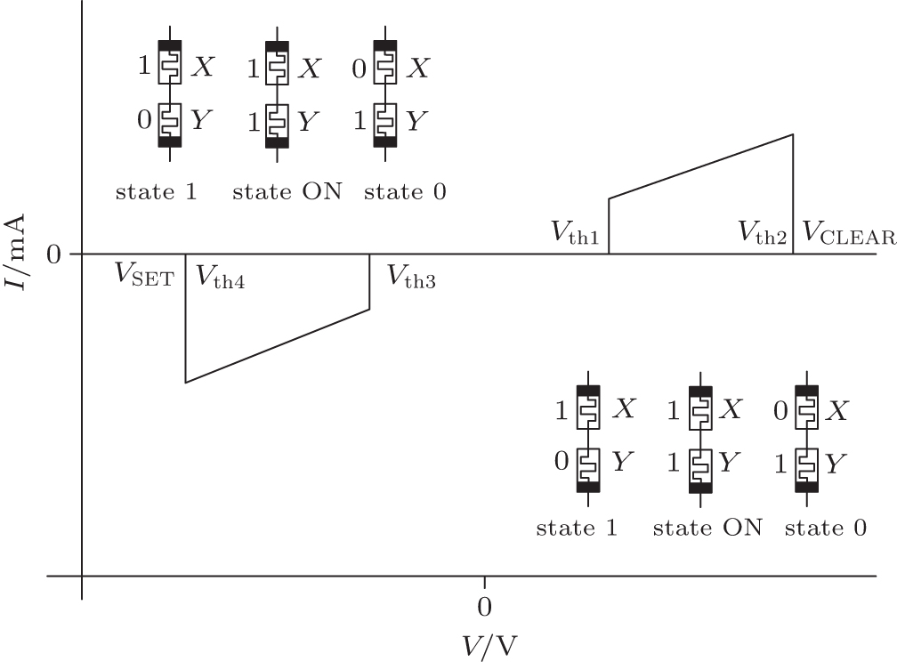
In addition, a memristor can be used in logic circuits,[13–15] logic arrays,[16–18] and other structures like CMOS-memristor hybrids.[19] Over the years, the memristor has been proposed as a replacement for the current CMOS-based memory architectures. For example, memristor-based crossbar arrays were used as feasible nonvolatile random access memories (RAMs) in Ref. [20]. However, passive crossbar arrays have the common problem about sneak path current due to interference from the neighboring cells when selecting a designated cell within the arrays.[21–23] Recently, the complementary resistive switch (CRS), which consists of two bipolar memristive elements anti-serially, was proposed to overcome the disadvantage of sneak path.[24] The element, including a high resistance state and a low resistance state, is used to encode either logic 0, 1, or ON state (see Fig. 1). If memristive element X is in the high resistance state (HRS), and memristive element Y is in the low resistance state (LRS), then CRS is in state 0. If memristive element X is in the LRS, and memristive element Y is in the HRS, then CRS is in state 1. If memristive elements X and Y are both in the LRS, then the CRS is in state ON. The transitions between these states depend on the applied biasing voltage across the CRS, controlled by Vth1, Vth2, Vth3, and Vth4 threshold voltages.[24]
Since Linn et al. proposed the CRS architecture in Ref. [24], many scholars have paid much attention to the CRS. In Ref. [15], Yang et al. proposed a scheme to implement the CRS-based stateful logic operations using material implication (IMP). However, during the IMP operation, the state 1 stored in the CRSP was reset to state 0, and for the NAND operation, the state 1 stored in the CRSP1 and CRSP2 was similarly reset to state 0. This scheme for the stateful logic operations partially destructs the original states stored in the input CRS cells. Moreover, the CRSs used in input and output cells are two different types of elements, then the configuration and parameter of input cell (CRSP) and output cell (CRSQ) are completely different. The output cell CRSQ can be only used as an output cell, which cannot be used as an input cell to perform the next logic operation, so it is hardly applied to massive passive crossbar arrays. In order to solve these issues, we put forward a circuit which consists of two parts including two CMOS switches, a resistor, and two voltage comparators. The circuit can be highly compatible with the CRS, and can be integrated to the peripheral circuit. The circuit will not bring extra area consumption of storage cells in massive passive crossbar arrays either. The main contributions of this paper are as follows.
The remainder of this paper is organized as follows. Section 2 presents our proposed circuit for CRS IMP, NAND operations and the CRS-based crossbar architecture with our proposed circuit. In Section 3, simulation results are provided to demonstrate the effectiveness and superior performance of the proposed circuit. Section 4 concludes this paper.
2. The proposed circuit and its applications to crossbar architectureIn this section, at first, we describe the CRS IMP operation using the proposed circuit. On this basis, we propose the CRS NAND operation. In order to apply CRS-based logic operations to crossbar arrays, we choose the same type of CRS as the CRSP and CRSQ. By implementing the two stateful logic operations, we show that our proposed circuit can perfectly address these problems existing in Ref. [15].
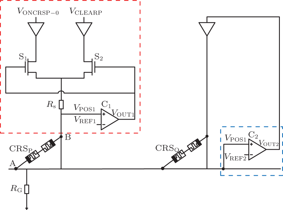
2.1. CRS IMP operation using our proposed circuitTo perform the CRS IMP operation using our proposed circuit, we consider the basic structure shown in Fig. 2.
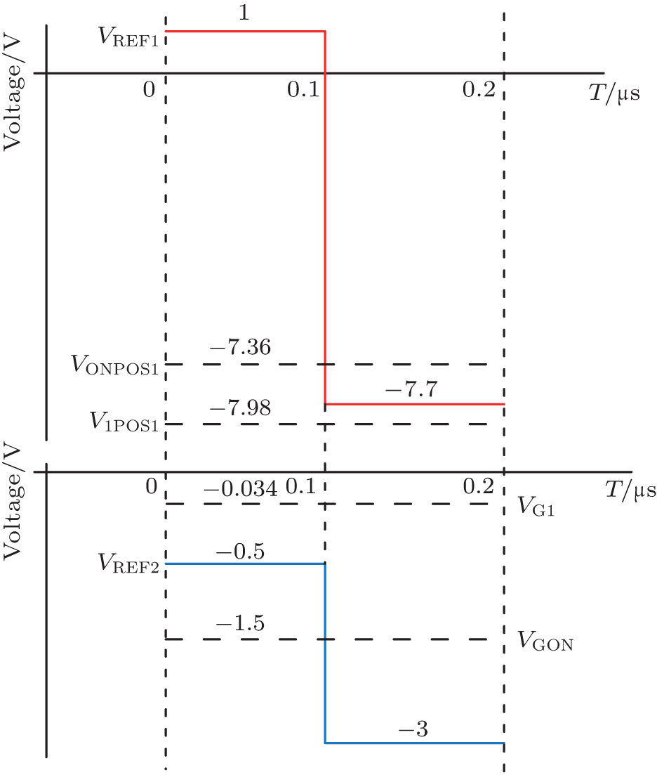
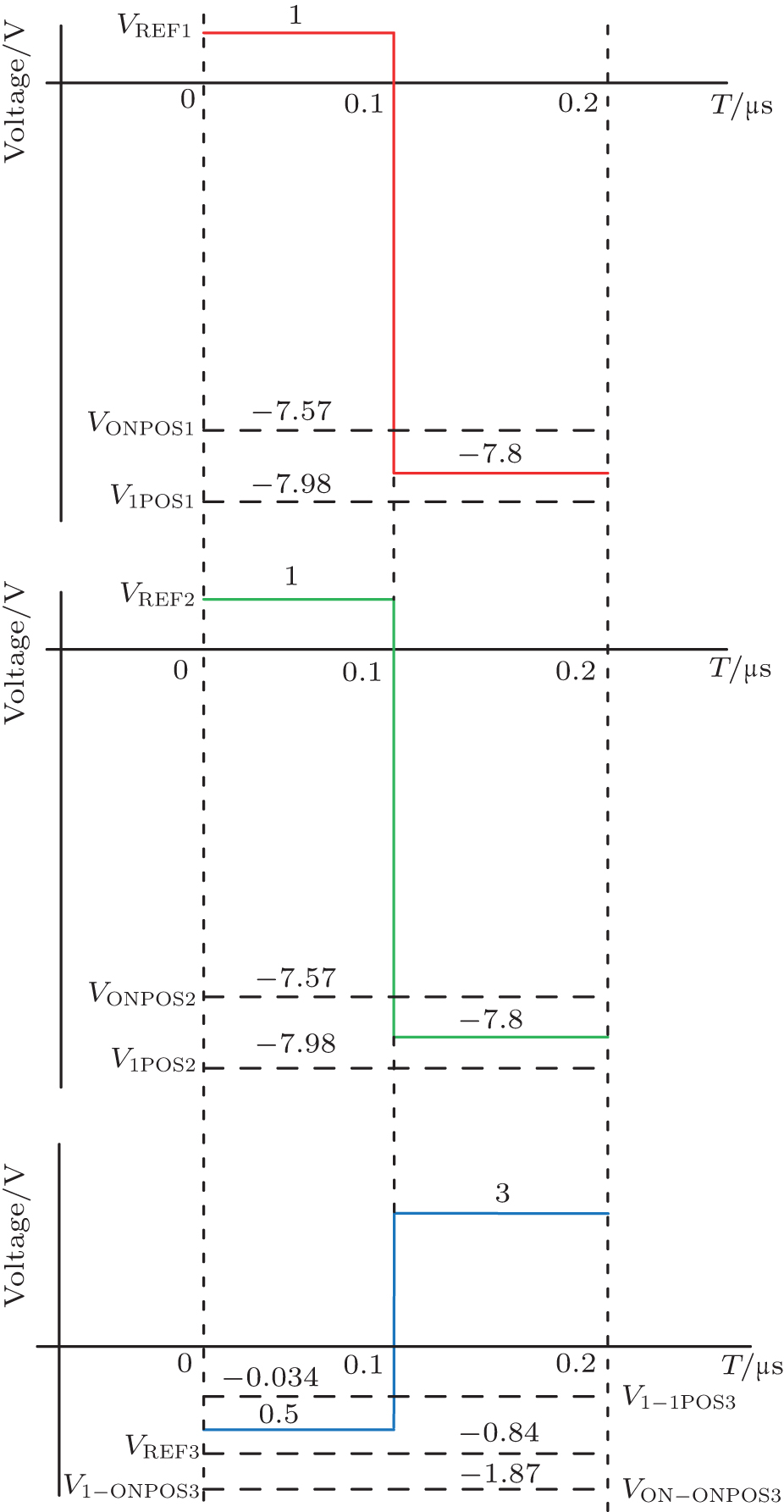
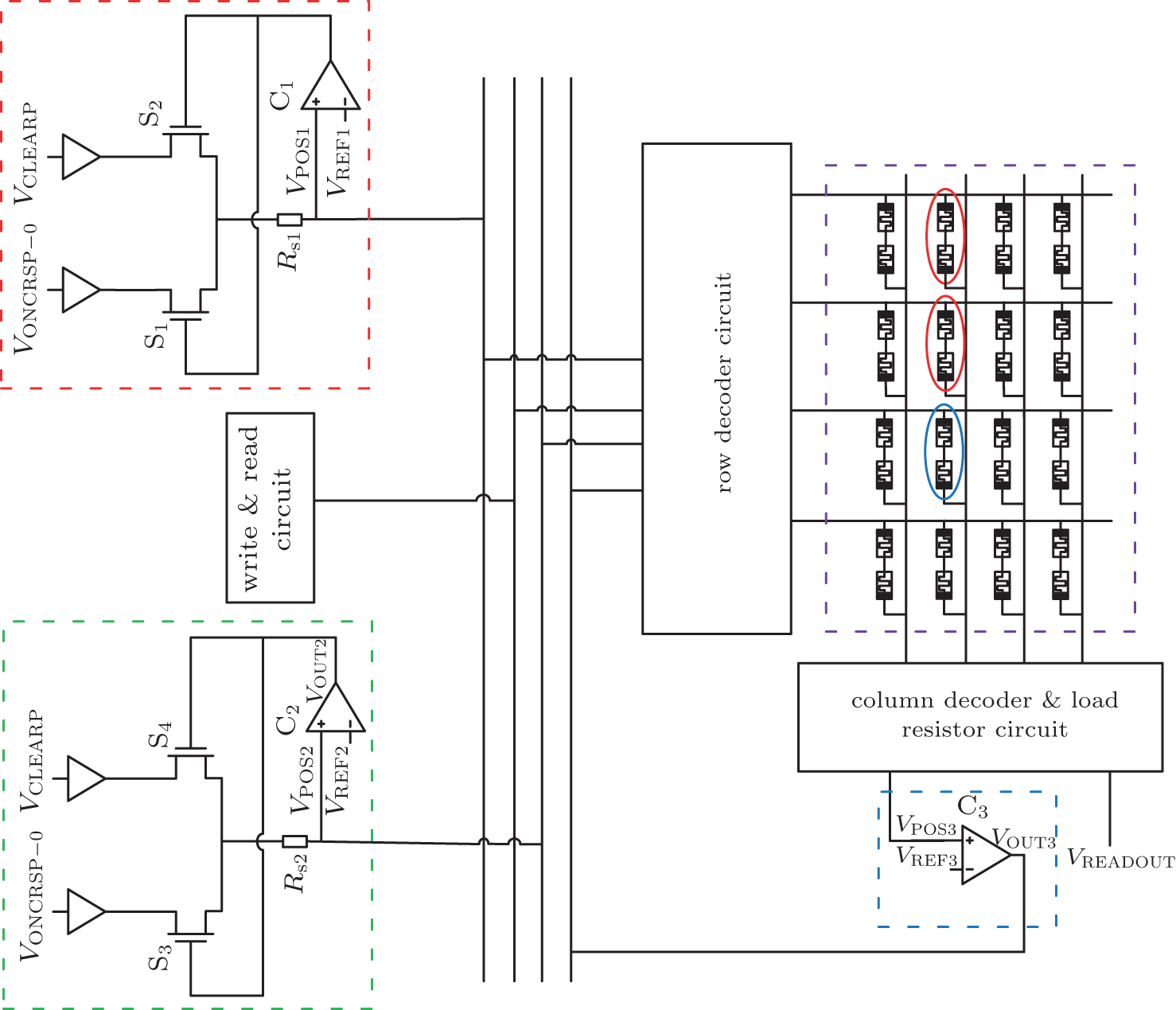
The circuits of red dashed line and blue dashed line present our proposed circuit. In the circuit of red dashed line, we adopt two CMOS switches S1 and S2, a voltage comparator C1, and a resistor RS of which resistance is fairly small compared with the resistance of CRSP state ON (RCRSONP). In the circuit of the blue dashed line, we only use a voltage comparator C2 to implement the related functions. In order to perform the CRS IMP operation using our proposed circuit, voltage VONCRSP–0 and VCLEARP are applied to switch S1 and S2. Voltage VONCRSP–0 is negative which can only switch CRSP from state 0 to state ON, and voltage VCLEARP is positive which resets CRSP to state 0. The output voltage of C1, namely VOUT1, is used to select switch S1 or S2. The S1 is a PMOS switch, and the S2 is a NMOS switch. When voltage VOUT1 is negative, switch S1 is turned on, S2 is turned off, and voltage VONCRSP–0 is applied to CRSP, resistor RS and RG. When voltage VOUT1 is positive, switch S2 is turned on, S1 is turned off, and voltage VCLEARP is applied to the circuit. Now, we show how the circuit in Fig. 2 is used to perform the IMP operation. At the beginning, voltage VPOS1 (positive terminal of C1) is equal to zero. We apply a positive pulse to voltage VREF1, and thus voltage VOUT1 will be negative, which turns on switch S1, imposes voltage VONCRSP–0 to the circuit. Under voltage VONCRSP–0, CRSP either stays in state 1 or switches from state 0 to state ON. The magnitude of the current passing through RS, CRSP, and RG when CRSP is in state ON is larger than the one when CRSP is in state 0. In order to perform CRS IMP operation correctly, the relationships of various operation voltages are given in Eqs. (1)–(3). When CRSP is in state ON, we define the potential of the node B (see Fig. 2) as VONPOS1, and we define the potential of the node A as VGON. When CRSP is in state 1, we define the potential of the node B as V1POS1, and we define the potential of the node A as VG1. Obviously, voltage VGON and VG1 meet Eq. (4). Similarly, the voltage drop over RS when CRSP is in state ON is much larger than the one when CRSP is in state 1. That is to say, voltage V1POS1 with CRSP staying in state 1 is less than VONPOS1 with CRSP staying in state ON, so voltage V1POS1 and VONPOS1 meet Eq. (5). Figure 3 presents the waveforms of the added voltage VREF1 and VREF2. Here, the proposed circuit is designed by using the parameters listed in Section 3. The voltages including VONPOS1, V1POS1, VG1, and VGON are measured in the circuit simulation, and the reference voltages, namely VREF1 and VREF2, are the added voltages.


where
VPth2,
VPth3, and
VPth4 are the threshold voltages of CRS
P,
VQth4 is the threshold voltage of CRS
Q,
V1POS1,
VONPOS1,
VGON, and
VG1 are all negative voltage. As shown in Fig.
3, in Step 1,
VREF1 is a positive voltage, and
RREF2 is negative which is larger than
VGON and less than
VG1. In Step 2, voltage
VREF1 is negative, which is larger than
V1POS1 and less than
VONPOS1; and voltage
RREF2 is also negative which is less than
VGON and
VG1. Now, we analyze the four input cases and the operation process.
Case 1 CRSP is in state 0, CRSQ is also in state 0. As shown in Fig. 3, firstly, voltage VREF1 is larger than VPOS1 which is about 0, and VOUT1 is negative which turns on S1. Then VONCRSP–0 is applied to the circuit (shown in Fig. 2). Under voltage VONCRSP–0, CRSP will be changed to state ON, then voltage VPOS2 is equal to VGON which is smaller than VREF2 (see Fig. 3). VOUT2 will be a negative voltage which is defined as VSETQ, and voltage VSETQ will set CRSQ to state 1. Secondly, when CRSP switches to state ON, VREF1 will be less than VONPOS1. In this way, switch S2 is turned on, and voltage VCLEARP will be applied to the circuit. Under voltage VCLEARP, CRSP will be changed from state ON to state 0. Note that voltage VCLEARP is positive. As a result, VPOS1 is also positive, switch S2 will be always turned on. VRG will be a small positive voltage, at the moment, we will apply a negative voltage to VREF2 (see Fig. 3). So VOUT2 will be a positive voltage which we define VLOW. Voltage VLOW is less than VQth1, which does not change the state of CRSQ, here, VQth1 is the threshold voltage of CRSQ, then CRSQ will still stay in state 1. After that, CRSP is in state 0, and CRSQ is changed to state 1.
Case 2 CRSP is in state 0, CRSQ is in state 1. Like Case 1, under VONCRSP–0, CRSP will be changed to state ON, then under voltage VCLEARP, CRSP will return to its original state (state 0). At the same time, CRSQ will not be changed. After that, CRSP is in state 0, CRSQ is in state 1.
Case 3 CRSP is in state 1, CRSQ is in state 0. Firstly, under voltage VONCRSP–0, CRSP remains in state 1, then voltage VPOS2 is equal to VG1 which is larger than VREF2, VOUT2 will not be equal to voltage VLOW which will not change the state of CRSQ. Secondly, when CRSP is in state 1 under voltage VONCRSP–0, VPOS1 is equal to V1POS1 which is less than voltage VREF1. Then VOUT1 is still negative, and switch S2 will not be turned on. In this way, voltage VPOS2 is still equal to VG1, which is still larger than VREF2. So, VOUT2 will still be equal to voltage VLOW which will not change the state of CRSQ. After that, CRSP is in state 1, CRSQ is in state 0.
Case 4 CRSP is in state 1, CRSQ is also in state 1. Like Case 3, under VONCRSP–0, CRSP remains in state 1. At the same time, CRSQ will not be changed. After that, CRSP is in state 1, CRSQ is in state 1.
The CRS IMP operation can be implemented using the proposed circuit during two steps. Table 1 presents the truth table, and Table 2 presents the applied voltages and steps of CRS IMP operation. In Section 3, we will present the simulation on CRS IMP operation, and the simulation result validates our proposed scheme.
Table 1.
Table 1.
 | Table 1. The truth table of CRS IMP operation. . |
Table 2.
Table 2.
Table 2. The operation voltages and steps of the CRS IMP operation. .
|
VP |
VQ |
Function |
| Step 1 |
VONCRSP–0 |
VSETQ |
Operation |
| (if CRSP is in state ON) |
| VLOW |
| (if CRSP is in state 1) |
| Step 2 |
VCLEARP |
|
Restoration |
| (if CRSP is in state ON) |
VLOW |
| VONCRSP–0 |
(less than VQth1) |
| (if CRSP is in state 1) |
|
| Table 2. The operation voltages and steps of the CRS IMP operation. . |
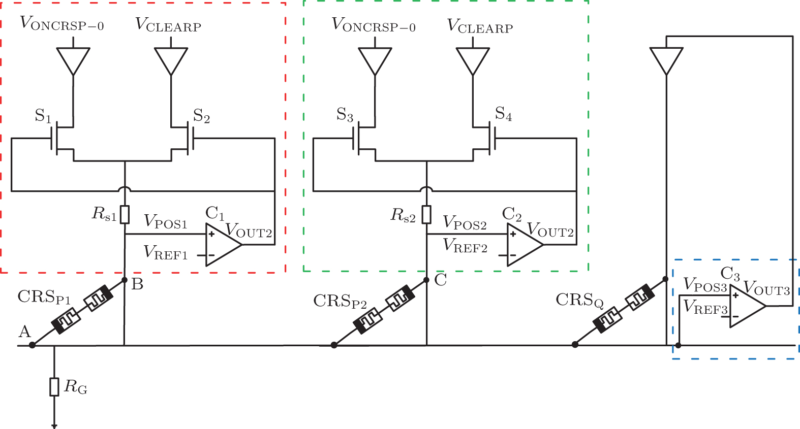
2.2. CRS NAND operation using our proposed circuitAccording to Ref. [13], any logic operation can be implemented using NAND gates. Hence, the following section will illustrate the details of CRS NAND operation. The two inputs NAND operation needs three CRS cells, CRSP1, CRSP2 (NAND inputs), and CRSQ which will store the result after NAND operation. Figure 4 presents the basic structure for performing the CRS NAND operation.
Like the CRS IMP operation, the circuits of red dashed line and green dashed line are added to CRSP1 and CRSP2 respectively, and the circuit of blue dashed line is used to drive CRSQ. The configuration and parameter in the circuits of red dashed line and green dashed line are completely the same. In order to describe the CRS NAND operation, we make some definitions. When CRSP1 is in state ON under voltage VONCRSP–0, we define the potential of the node B as VONPOS1 (see Fig. 4). When CRSP1 is still in state 1 under voltage VONCRSP–0, we define the potential of the node B as V1POS1. Similarly, we can define VONPOS2 and V1POS2. When CRSP1 and CRSP2 are both in state 1 under voltage VONCRSP–0, we define the potential of the node A as V1–1POS3. When one of CRSP1 and CRSP2 is in state ON and the other is in state 1 under voltage VONCRSP–0, we define the potential of the node A as V1–ONPOS3. When CRSP1 and CRSP2 are both in state ON under voltage VONCRSP–0, we define the potential of the node A as VON–ONPOS3. Apparently, equations (7)–(9) are all satisfied. Figure 5 presents the waveforms of the added voltage VREF1, VREF2, and VREF3. Here, like the CRS IMP operation, the proposed circuit is also designed by using the parameters listed in Section 3. The voltages including VONPOS1, V1POS1, VONPOS2, V1POS2, V1–1POS3, V1–ONPOS3, and VON–ONPOS3 are measured in the circuit simulation, and the reference voltages, namely VREF1, VREF2, and VREF3 are the added voltages.


where
VQth2 is the threshold voltage of CRS
Q, voltage
VONPOS1,
VONPOS2, and
V1–1POS3 are all negative. To implement the CRS NAND operation, in Step 1, we apply voltage
VSETQ to CRS
Q, which sets CRS
Q to state 1 unconditionally. Then we remove voltage
VSETQ. Considering Fig.
5, in Step 2, for the fact that voltages
VPOS1 and
VPOS2 are about 0, we apply a positive voltage to
VREF1 and
VREF2, then
VOUT1 and
VOUT2 are negative and will turn on switch S
1 and S
3, so voltage
VONCRSP–0 will be added to the circuit. At the same time, a negative voltage is applied to
VREF3 which is larger than
V1–ONPOS3,
VON–ONPOS3, and less than
V1–1POS3. In Step 3, we apply a negative voltage to
VREF1 which is larger than
V1POS1 and less than
VONPOS1, and it is the same as voltage
VREF2. In the meantime, a positive voltage is applied to
VREF3 which is larger than
VPOS3. Now, we analyze the four input cases and the operation process.
Case 1 CRSP1 is in state 0, and CRSP2 is also in state 0. Firstly, voltage VSETQ sets CRSQ state 1, then voltage VONCRSP–0 is added to the circuit, CRSP1 and CRSP2 will be changed to state ON under voltage VONCRSP–0. At the same time, the added voltage VREF3 is larger than VON–ONPOS3, then voltage VOUT3 is a negative voltage which we define as VQLOW. The magnitude of VQLOW is less than VQth3, which will not change the state of CRSQ, here, VQth3 is the threshold voltage of CRSQ. Secondly, the added negative voltage VREF1 and VREF2 are less than VONPOS1 and VONPOS2, respectively. So, voltage VOUT1 and VOUT2 are positive which will turn on switch S2 and S4, voltage VCLEARP is added to the circuit. Under voltage VCLEARP, CRSP1 and CRSP2 will be reset to state 0, and voltage VPOS1 and VPOS2 will be positive which are larger than VREF1 and VREF2 respectively, switch S1 and S3 will not be always turned on, therefore CRSP1 and CRSP2 will remain in state 0. However, biased by voltage VCLEARP, VPOS3 is a small positive voltage. So we apply an appropriate positive voltage to VREF3 which is larger than VPOS3, the voltage VOUT3 is equal to VQLOW which will not change the state of CRSQ. In this way, CRSQ is still in state 1. After that, CRSP1 is in state 0, CRSP2 is in state 0, and CRSQ is in state 1.
Case 2 CRSP1 is in state 0, CRSP2 is in state 1. Firstly, voltage VSETQ sets CRSQ state 1, then voltage VONCRSP–0 is added to the circuit. Under voltage VONCRSP–0, CRSP1 will switch to state ON, while CRSP2 keeps the state. Voltage VPOS3 is V1–ONPOS3, while the added voltage VREF3 is larger than V1–ONPOS3, so voltage VOUT3 is equal to VQLOW which will not change the state of CRSQ. Secondly, the added negative voltage VREF1 is less than VONPOS1, then switch S2 will be turned on, so CRSP1 will be reset to state 0 biased by voltage VCLEARP. For the fact that the added negative voltage VREF2 is larger than V1POS2, then switch S4 will not be turned on, so the state of CRSP2 will not be changed. While biased by voltage VONCRSP–0 and VCLEARP, VPOS3 is a small positive voltage. Like Case 1, we apply the same voltage to VREF3 which is larger than VPOS3. In this way, CRSQ is still in state 1. After that, CRSP1 is in state 0, CRSP2 is in state 1, and CRSQ is in state 1.
Case 3 CRSP1 is in state 1, CRSP2 is in state 0. Case 3 is the same as Case 2. After that, CRSP1 is in state 1, CRSP2 is in state 0, and CRSQ is in state 1.
Case 4 CRSP1 is in state 1, CRSP2 is also in state 1. Firstly, voltage VSETQ sets CRSQ to state 1, then voltage VONCRSP–0 is added to the circuit. Under voltage VONCRSP–0, CRSP1 and CRSP2 will keep the state. In the meantime, voltage VPOS3 is equal to V1–1POS3, and voltage VREF3 is less than V1–1POS3 (shown in Fig. 5), which makes comparator C3 output a positive voltage. Here, we define the positive voltage VCLEARQ, which can reset CRSQ to state 0. Secondly, the added negative voltage VREF1 and VREF2 are larger than V1POS1 and V1POS2, respectively. So, voltage VOUT1 and VOUT2 are negative which will not turn on switch S2 and S4, and voltage VCLEARP will not be added to the circuit. At the same time, the added positive voltage VREF3 is larger than V1–1POS3. The voltage VOUT3 is equal to VQLOW which will not change the state of CRSQ. After that, CRSP1 is in state 1, CRSP2 is in state 1, and CRSQ is in state 0.
The CRS NAND operation can be implemented using the proposed circuit during three steps. Table 3 presents the truth table, and Table 4 presents the operation voltages and steps of CRS NAND operation. In Section 3, we will show the simulation on CRS NAND operation, and the simulation result validates our proposed scheme.
Table 3.
Table 3.
| Table 3. The truth table of CRS NAND operation. . |
Table 4.
Table 4.
Table 4. The operation voltages and steps of the CRS NAND operation. .
|
VP1 |
VP2 |
VQ |
Function |
| Step 1 |
− |
– |
VSETQ |
Initialization |
| Step 2 |
VONCRSP–0 |
VONCRSP–0 |
VCLEARQ(CRSP1 = state 1,CRSP2 = state 1)VQLOW(other cases,larger than VQth3 |
Operation |
| Step 3 |
VONCRSP–0 |
VONCRSP–0 |
|
Restoration |
| (CRSP1 = state 1) |
(CRSP2 = state 1) |
VQLOW |
| VCLEARP |
VCLEARP |
(larger than VQth3) |
| (CRSP1 = state ON) |
(CRSP2 = state ON) |
| Table 4. The operation voltages and steps of the CRS NAND operation. . |
To perform N inputs CRS NAND operation, we need N + 1 CRS cells to achieve the function, in which N CRS cells are used for N inputs cells, and the other is considered as the output cell. It needs only three steps. In Step 1, CRSQ is initialized to state 1, then N inputs CRS NAND operation can be executed by two steps using our proposed circuit. For the CRS NAND operation in Ref. [10], it needs four steps. For memristor NAND operation in the previous literature, it needs N times IMP, so N inputs memristor NAND operation requires N + 1 steps (N IMP steps plus one initialization). The comparison about steps of IMP and NAND operations is shown in Table 5.
Table 5.
Table 5.
Table 5. Comparison about steps of IMP and NAND operations. .
| Logic operation |
Implementation steps |
|
CRS using ourproposed circuit |
CRS[15] |
Memristor[13,14] |
| IMP |
2 |
3 |
1 |
| 2 inputs NAND |
3 |
4 |
3 |
| 3 inputs NAND |
3 |
4 |
4 |
| 4 inputs NAND |
3 |
4 |
5 |
| N inputs NAND |
3 |
4 |
N + 1 |
| Table 5. Comparison about steps of IMP and NAND operations. . |
2.3. CRS-based crossbar architecture with our proposed circuitIn the preliminary, we have already implemented the two foremost CRS logic operations. According to Ref. [13], any logic operation can be performed using the NAND gates. In addition, other stateful logic operations can be also implemented using our proposed circuit. We will apply the CRS NAND operation with our proposed circuit to crossbar architecture. Figure 6 shows the basic structure. In Fig. 6, the circuits of red, green, and blue dashed line present our proposed circuit. The row decoder circuit, column decoder, and load resistor circuit are used to choose the selected row and column. To perform the CRS NAND operation in crossbar arrays, we take 4 × 4 crossbar arrays for example. The three rows in front are selected, and the second column is selected. In this way, the two red circled CRS cells are used as the input cells, and the blue circled CRS cell is considered as output cell. According to the operation steps presented in Section 2.2, we can implement the CRS NAND operation in crossbar arrays. We can also write and read any CRS cell in crossbar arrays using the write and read circuits (see Fig. 6). Not only CRS NAND operation can be performed, but also other CRS operations, such as CRS IMP, CRS NOR operations, and so on, can be implemented in the crossbar arrays.
3. Simulation resultsThe following presents the simulation results of CRS IMP and NAND operations using Hspice simulation tool. To perform the CRS stateful logic operations, the parameters of CRS cells should satisfy Eqs. (1)–(3), and (6). Here, for CRSP and CRSQ, we choose RON = 100 Ω for state ON of memristive elements X and Y, and ROFF = 10 kΩ for state OFF of memristive elements X and Y. In this way, we can ensure the same configuration and parameter of CRSP and CRSQ, which can be applied to massive crossbar arrays better. Moreover, we select RG = 50 Ω and RS = 20 Ω. We use −12 V for VSETQ, 12 V for VCLEARP and VCLEARQ. According to Eq. (1), VONCRSP–0 is −8 V.
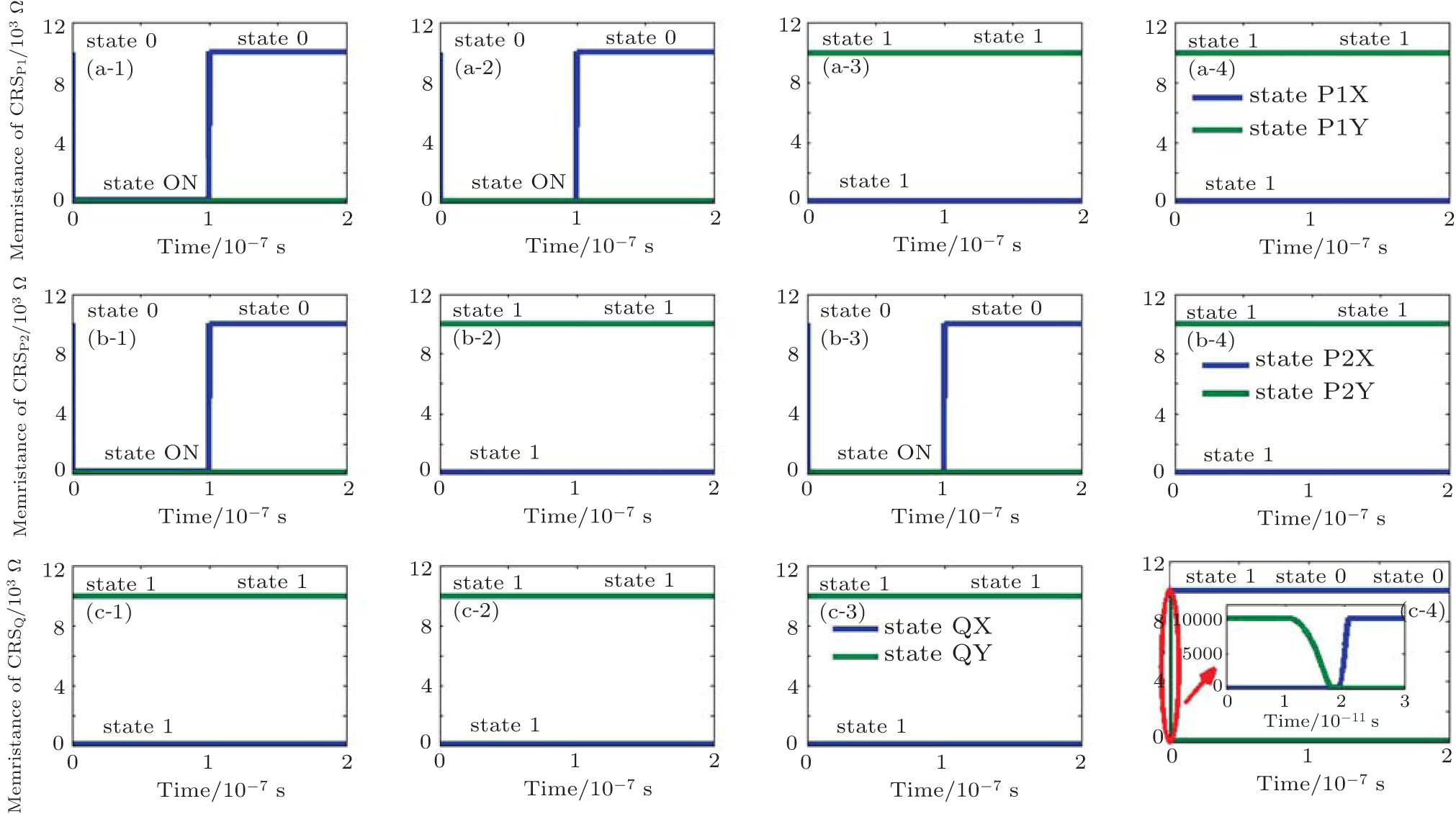
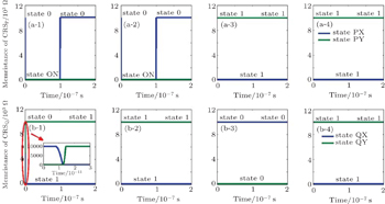
3.1. Simulation on CRS IMP operationFigure 7 shows the CRS IMP operation simulation results. In Figs. 7(a) and 7(b), the states of CRSP and CRSQ are represented by two memristive elements which are called state PX, state QX (blue bold line) and state PY, state QY (green bold line), respectively. As shown in Fig. 7, there are three states for CRSP and CRSQ. The first state is the original state. After Step 1, CRSP and CRSQ switch to the second state, and after Step 2, CRSP and CRSQ switch to the third state. Now, we take Case 1 for example. The original states of CRSP and CRSQ are state 0. After Step 1, CRSP switches to state ON, while CRSQ switches to state 1. After Step 2, CRSP switches to state 0, while CRSQ remains unchanged. After that, the state of CRSQ is the result of IMP operation, and CRSP remains in its original state, which is not destroyed. It is the same as the other three cases (see Fig. 7). The simulation results validate our proposed scheme.
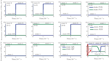
3.2. Simulation on CRS NAND operationFigure 8 shows the simulated results of the CRS NAND operation circuit (see Fig. 4). Like the CRS IMP operation, there are three states for CRSP1, CRSP2, and CRSQ (see Fig. 8). The first states of CRSP1 and CRSP2 are the original states, and the first state of CRSQ is the initialized state. During Step 1, CRSQ is initialized to state 1. After Step 2, CRSP1, CRSP2, and CRSQ switch to the second state, and after Step 3, CRSP1, CRSP2, and CRSQ switch to the third state. Now, we take Case 1 for example. The original states of CRSP1 and CRSP2 are state 0. During Step 1, CRSQ is initialized to state 1. After Step 2, CRSP1 and CRSP2 both switch to state ON, and CRSQ remains in state 1. After Step 3, CRSP1 and CRSP2 both switch from state ON to state 0, and CRSQ still remains in state 1. After that, the state of CRSQ is the result of NAND operation, CRSP1 and CRSP2 remain in their original states, which are not destroyed. It is the same as the other three cases (see Fig. 8). The simulation results validate our proposed scheme.


 , Chen Lin1, 2, Shen Yi1, 2, Xu Bo-Wen1, 2]