Hou Xiao-Hui, Zheng Xue-Feng, Wang Ao-Chen, Wang Ying-Zhe, Wen Hao-Yu, Liu Zhi-Jing, Li Xiao-Wei, Wu Yin-He. Distribution of electron traps in SiO2/HfO2 nMOSFET. Chinese Physics B, 2016, 25(5): 057702
Permissions
Distribution of electron traps in SiO2/HfO2 nMOSFET
Hou Xiao-Hui1, Zheng Xue-Feng2, †, , Wang Ao-Chen2, Wang Ying-Zhe2, Wen Hao-Yu2, Liu Zhi-Jing1, Li Xiao-Wei2, Wu Yin-He2
School of Computer Science, Xidian University, Xi’an 710071, China
Key Laboratory of Wide Bandgap Semiconductor Materials and Devices, School of Microelectronics, Xidian University, Xi’an 710071, China
Project supported by the National Natural Science Foundation of China (Grant Nos. 61334002, 61106106, and 61474091), the New Experiment Development Funds for Xidian University, China (Grant No. SY1434), and the Scientific Research Foundation for the Returned Overseas Chinese Scholars, State Education Ministry, China (Grant No. JY0600132501).
Abstract
Abstract
In this paper, the principle of discharge-based pulsed I–V technique is introduced. By using it, the energy and spatial distributions of electron traps within the 4-nm HfO2 layer have been extracted. Two peaks are observed, which are located at ΔE ∼ −1.0 eV and −1.43 eV, respectively. It is found that the former one is close to the SiO2/HfO2 interface and the latter one is close to the gate electrode. It is also observed that the maximum discharge time has little effect on the energy distribution. Finally, the impact of electrical stress on the HfO2 layer is also studied. During stress, no new electron traps and interface states are generated. Meanwhile, the electrical stress also has no impact on the energy and spatial distribution of as-grown traps. The results provide valuable information for theoretical modeling establishment, material assessment, and reliability improvement for advanced semiconductor devices.
In order to realize the aggressively continuous downscaling of CMOS technology, high-k materials are important approaches. With the aid of high-k materials, a small equivalent oxide thickness (EOT) can be realized even under a thick physical thickness, which can decrease the static power dissipation in integrated circuits and improve the data retention in Flash memory.[1–3] Meanwhile, high-k materials are also used in III–V high electron mobility transistors (HEMTs) to replace the conventional Schottky gate. By utilizing it, the gate leakage current can be decreased, which can improve the breakdown voltage, power added efficiency, and long-term reliability.[4,5] Nowadays, high-k materials are becoming more and more important in semiconductor devices.
Besides the regular Al2O3 dielectric, HfO2 is also considered as a good high-k material due to the relatively high dielectric constant, good thermal stability, etc.[6] Generally, the quality of high-k is not so good as that of mature SiOxNy dielectric. Previous works have demonstrated that there are large densities of pre-existing traps in HfO2,[7,8] which are a few orders of magnitude higher than that in SiO2. It has become a bottleneck that hinders the wide application of high-k materials and improvement of long-term reliability. Therefore, in-depth understanding on the properties of traps in HfO2 becomes an important issue. Among it, the energy and spatial distribution of electron traps within HfO2 is a major concern, which plays a vital role in theoretical modeling establishment and material assessment. Early works on trap distribution study were mainly based on the numerical calculation.[9,10] However, direct experimental evidence is still rather limited.
There are two obstacles that limit the in-depth experimental study on electron traps in HfO2. Firstly, the trapped electron in HfO2 can be easily discharged. Conventional C–V/I–V techniques, which feature the measurement speed of 10 s, are too slow to correctly measure the defects due to the fast discharging in HfO2. Secondly, the existing characterization techniques for electron trap energy distribution have obvious limitations. For example, the advanced charge-pumping technique can only detect the electron traps which are at about 1 nm in the high-k layer, due to the minimum frequency being limited at around 100 Hz.[2,11] The charge injection and sensing (CIS) technique can detect the traps at about 2–3 nm within the high-k layer. This region, however, is still very limited in comparison with the entire high-k layer.[12] Then most of the electron traps within the high-k layer can still not be detected. To overcome it, we developed a discharge-based multi-pulse technique,[13,14] and the electron trap energy distribution within HfO2 has been discussed. However, the spatial distribution has not been discussed. Furthermore, the impact of electrical stress on electron traps has not been explored.
In this work, the principle of our developed discharge-based pulsed I–V technique will be briefly introduced. With the aid of it, the energy and spatial distributions of electron traps within the HfO2 layer have been extracted. The effect of discharge time on the electron trap distribution is also discussed. Furthermore, the influence of electrical stress on electron traps within HfO2 and interface states at the substrate/gate dielectric are investigated as well. The above works provide valuable information for theoretical modeling estimation, material and processing assessment, and reliability improvement in advanced semiconductor devices.
2. Devices and experiments
The devices used in this paper are nMOSFETs that are fabricated on p-type Si wafer. The gate dielectric consists of 1-nm SiO2 and 4-nm HfO2, which is deposited by atomic layer deposition. The detailed process information can be found in Ref. [13]. By using the HP 4156B semiconductor parameter analyzer, the conventional DC Id−Vg curve of the nMOSFET is shown in Fig. 1. The interface state density is about 2.8× 1010 cm−2. Furthermore, the difference between devices is negligible.
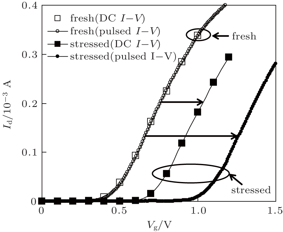
Fig. 1. The Id–Vg curves measured by the DC I–V technique and pulsed I–V technique before and after stress on a fresh device, respectively. The stress is 2.1 V for 10 s.
It is known that fast detrapping exists in MOSFETs with HfO2 gate dielectric. In this paper, a pulsed I–V technique is used to measure the transfer characteristics (Id–Vg) of devices.[15] It can significantly shorten the measurement period, and improve the measurement accuracy accordingly. The pulse measurement system consists of a pulse generator, oscilloscope and current–voltage amplifier,[15] which can obtain the transfer characteristics within 5 μs in this paper. For the conventional DC I–V technique, it is about 10 s. The Id–Vg curves measured by pulsed technique on the identical fresh device are also presented in Fig. 1. It is evident that these two curves overlap well, which demonstrates that the measurement results by the pulsed I–V are reliable.
Furthermore, the effect of the measurement technique was also studied in this paper. A stress of 2.1 V for 10 s was applied on a fresh device. After the stress, the conventional DC I–V and pulsed I–V were carried out immediately to obtain the Id–Vg curves. As shown in Fig. 1, both of these two curves shift positively compared to that on a fresh device, which demonstrates that significant electron trapping in HfO2 occurs during stress. However, the shift measured by pulsed I–V is much larger. It can be explained by the longer measurement period by DC I–V, during which significant trapped electrons in HfO2 are discharged. Accordingly, the results measured by conventional DC I–V will underestimate the electron trapping in high-k layers.
Considering the above advantages, the pulsed I–V technique becomes very important for accurate characterization of the trapping and detrapping in a device with HfO2 gate dielectric. In this paper, the effective trap density can be obtained by the shift of threshold voltage, ΔVth. For data process simplicity, the threshold voltage is extracted from the Id–Vg curve at a constant drain current of 10−4 A with a drain bias of 100 mV.
3. Results and discussion
To probe the electron trap energy distribution, we developed a discharge-based pulsed I–V technique. The principle will be introduced briefly as follows.
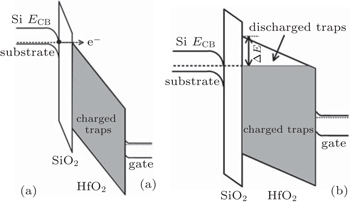
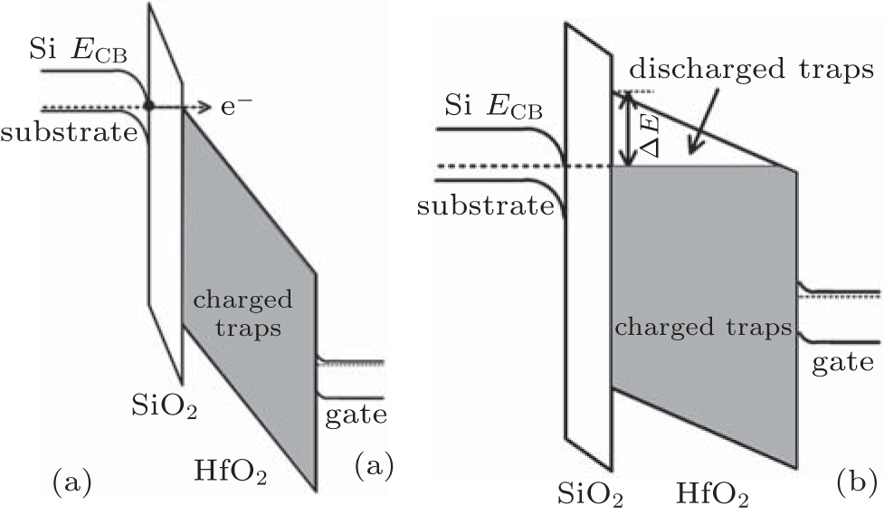
Firstly, the entire electron traps within the HfO2 layer will be charged by applying a high positive bias on the gate. As shown in Fig. 2(a), the electrons can be injected into the conduction band of the high-k layer from Si conduction band bottom (ECB) and fill the empty traps within the high-k layer via scattering. Secondly, a lower bias is then applied on the gate immediately for detrapping. As shown in Fig. 2(b), the trapped electrons within the empty region in HfO2 are above the Si ECB and can be discharged. When the electrons within this region are totally discharged, the gate bias will be lowered further, and the electrons within a deeper energy level can be discharged. By repeating the above process via reducing the gate bias, all trapped electrons within HfO2 can be detected.
Fig. 2. The schematic energy band diagrams of nMOSFET with SiO2/HfO2 gate dielectric for (a) charging at high positive gate bias and (b) discharging at lower gate bias, respectively.
During the above process, the following respects should be noted: (I) pulsed I–V is used to monitor the Vth at the pre-set time, which is to ensure that the discharge is saturated; (II) during discharge, the discharge time should be long enough to ensure that all electron traps are discharged; (III) the gate bias for charge or discharge should be safe, i.e., new electron traps or interface states should not be generated during these processes; (IV) the time interval between the two consecutive process, such as charge and discharge, should be minimized to zero to avoid the undesired detrapping. With the aid of a pulse generator, it can be easily realized. However, it cannot be easily realized in a conventional DC measurement system; (V) ΔE, as shown in Fig. 2(b), represents the energy level offset between the Si ECB and the conduction band of HfO2 at the SiO2/HfO2 interface under the gate bias of Vg. It demonstrates the energy region of electron traps that can be discharged in HfO2, which is strongly related to the gate bias and can be calculated according to the following expression:[11]
where ΔEC(HfO2−Si) is a constant and represents the conduction band bottom offset between HfO2 and Si substrate at the flat band state, VFB is the flat band voltage, Φs represents the surface potential in the substrate and poly gate electrode, which is strongly related to the gate bias, εHfO2 and εSiO2 are the permittivity of HfO2 and SiO2, respectively. tHfO2 and tSiO2 are the permittivity of HfO2 and SiO2, respectively.
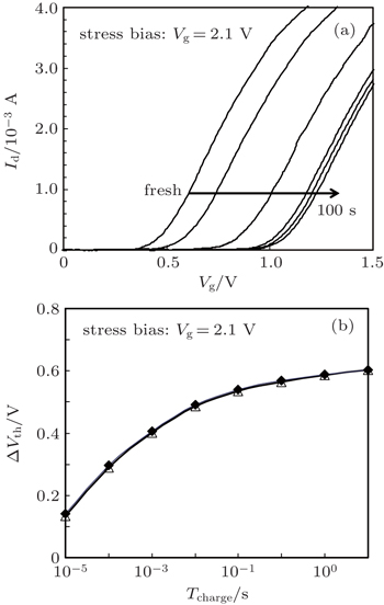
In this paper, the gate bias for filling the empty electron traps is selected as Vg = 2.1 V, which is high enough to fill the electron traps with a shallow energy level in the HfO2 layer. Figure 3(a) presents the pulsed Id–Vg curves that were obtained at different times under the bias of 2.1 V. It is clearly observed that the pulsed I–V curve shifts positively with the increasing charge time. Figure 3(b) shows the shift of threshold voltage, ΔVth, versus the charge time, which indicates that there are significant electron traps within the HfO2. Most of the electron traps can be charged when the filling time is increased to 10 s. One concern is whether they are as-grown electron traps or newly generated. To explore this question, a high negative gate bias is applied on the above device for a long time to discharge all the trapped electrons. Then a bias of 2.1 V is applied on the gate of this device again. As shown in Fig. 3(b), it is observed that the curves before and after the discharge agree well, indicating that the bias of 2.1 V for 10 s does not generate any new electron traps, i.e., all the traps that we study here are as-grown electron traps.
Fig. 3. (a) The Id–Vg curves measured by pulsed I–V technique with different charge time. (b) The shift of threshold voltage, ΔVth, versus charge time before and after stress, respectively. The stress bias is of 2.1 V.
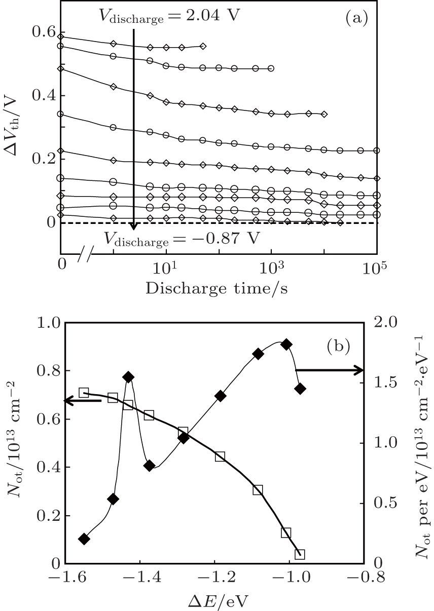
After the filling, the gate bias is immediately switched to a series of lower gate bias sequentially for discharging. Figure 4(a) shows the shift of threshold voltage versus discharge time during discharging. It should be noted that the maximum discharge time is 100 ks here to ensure all the electrons can be discharged. It is evident that the electrons trapped in a shallower energy region are easily discharged, which is less than 1 ks. Eventually, all the trapped electrons can be discharged, indicating all the electron traps within HfO2 can be sensed using this technique. Instead of it, the techniques in previous works can only probe the traps within a limited region.[2,12] The accumulative discharged electron trap density, Not, versus ΔE is extracted and shown in Fig. 4(b). It is clear that the electrons in the shallower energy region have a high percent. To quantitatively characterize it, the trap density per electronvolt versus ΔE is also presented. Two peaks can be observed. For the electron traps with ΔE ∼ −1.0 eV, it can be referred to as shallow traps, which is slightly different with ΔE ∼ −1.1 eV that was observed by Cartier using an advanced charge pumping technique.[16] It may be explained by the different sample that we used in this work. It should also be noted that the electron trap region that we detected is much wider than that by Cartier. These shallow traps correspond to the fast charging or discharging, and cannot be accurately measured using conventional techniques as that in Fig. 1. For the electron traps with ΔE ∼ −1.43 eV, it is generally referred to as deep traps. In early work, it has been obtained according to the calculation.[17] Our work confirms it by direct experimental evidence. Furthermore, the detailed trap density across the bandgap of HfO2 is also provided in this work. According to previous works, these as-grown traps are classified as oxygen vacancies and the post-gate annealing process is used to minimize their effect.[9,10]
Fig. 4. (a)ΔVth versus discharge time during the discharging period under different biases. The Vth is measured by pulsed I–V technique at pre-set interval. (b) The accumulative discharged electron trap density and trap density per electronvolt versus ΔE, respectively. The maximum discharge time is 100 ks.
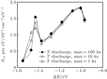
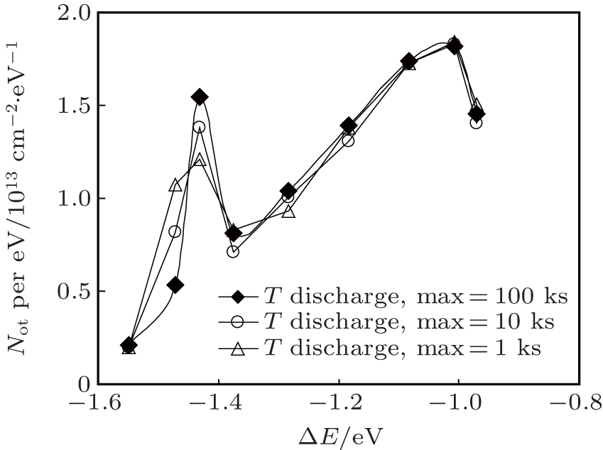
It should be noted that the maximum discharge time used above is 100 ks. Although it can improve the accuracy of characterization, however, it is very time-consuming. In order to investigate the effect of discharge time on electron trap energy distribution, the maximum discharge time is decreased to 10 ks and 1 ks, respectively. The energy distribution results are presented in Fig. 5. It is clearly observed that the discharge time has little effect on the energy location of electron traps in HfO2. For the peak value of deep traps, it increases with the increasing discharge time. It can be explained by that more electrons are discharged with longer discharging time. Then, we may conclude that the results under 1 ks can be used for a rapid energy distribution evaluation. However, for accurate evaluation, the maximum discharge time should be increased to 100 ks in 4-nm HfO2.
Fig. 5. The trap density per electronvolt versus ΔE with different discharge time. The maximum discharge times are 100 ks, 10 ks and 1 ks, respectively. The charge bias is 2.1 V for 10 s.
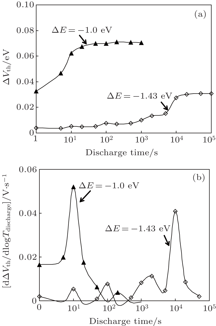
Besides the energy distribution, the spatial distribution of electron traps within HfO2 is also eagerly required during theoretical modeling, etc. Generally, the calculation for spatial distribution is very complex. According to the tunneling theory, a longer discharge time corresponds to discharge traps farther away from the substrate. Figure 6(a) presents the shift of threshold voltage versus discharge time for electron traps with ΔE ∼ −1.0 eV and −1.43 eV, respectively. Both of these two curves have a sharp increase, indicating the high density of electron traps with HfO2. In order to have an in-depth spatial distribution investigation, the curves of dΔVth/d log Tdischarge versus discharge time are calculated and shown in Fig. 6(b). Both of these two curves have a peak, which indicates that the electron traps are not uniformly distributed in the HfO2 layer. For the traps with ΔE ∼ −1.0 eV, the peak is located at about 10 s, which indicates that the shallow traps are close to the SiO2/HfO2 interface. It is known that there is a transition region between SiO2 and HfO2, where the microstructure at this region is clearly different from that in HfO2.[18] This transition region is expected to be the origin of the sharp increase of electron traps. In addition, the value of this peak can be used to evaluate the interface quality between SiO2 and HfO2. However, for the traps with ΔE ∼ −1.43 eV, the peak is located at about 10 ks, which indicates that the deep traps are located far away from the SiO2/HfO2 interface and close to the gate electrode. In previous works, such as the advanced charge pumping technique,[2,19] the maximum discharge time is limited to 10 ms. Then the electron traps close to the gate electrode cannot be observed. Instead of it, our technique provides a powerful tool to probe the traps near the gate electrode. Therefore, the maximum discharge time should be long enough for spatial distribution extraction.
Fig. 6. (a) The ΔVth versus discharge time and (b) dΔVth/d log Tdischarge versus discharge time at ΔE ∼ −1.0 eV and −1.43 eV, respectively. The charging bias is 2.1 V for 10 s. The maximum discharge time is 100 ks.
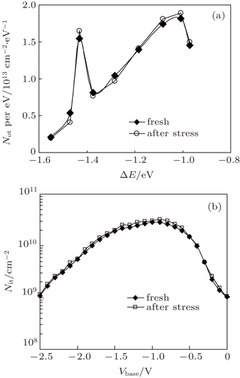
Note that the above investigations are focused on the as-grown electron traps in HfO2. To the best of our knowledge, little study has been paid on the newly generated electron traps under electrical stress. In order to investigate it, a high positive bias of 3.0 V for 100 s is applied on the gate of the device. Following the stress, the discharge-based pulsed technique is carried out. Figure 7(a) shows the energy distribution of electron traps within HfO2 before and after the above electrical stress. It is evident that there is no significant difference between them. Meanwhile, the spatial distributions with and without the stress are also compared and no significant difference is observed, which is not shown here. Then it indicates that the electrical stress will not generate any new electron traps in HfO2 and it also has little effect on the distribution of as-grown traps. Furthermore, the interface states with and without the stress are also studied via the charge-pumping technique. As shown in Fig. 7(b), the stress has a negligible effect on the interface states as well. The above results support that the as-grown electrons in HfO2 play an important role in device performance.
Fig. 7. (a) The energy distribution of electron traps and (b) charge-pumping curves before and after electrical stress, respectively. The electrical stress is of 3.0 V for 100 s and the maximum discharge time is 100 ks.
4. Conclusions
In this paper, the energy and spatial distributions of electron traps within the 4-nm HfO2 layer have been investigated. By using the discharge-based pulsed I–V technique, it is found that there are two peaks existing in HfO2, which are located at ΔE ∼ −1.0 eV and −1.43 eV, respectively. The former one is close to the SiO2/HfO2 interface, however, the latter one is close to the gate electrode. Finally, the effect of electrical stress on the distribution of electron traps has also been studied. During stress, there is no additional electron traps and interface states are newly generated. The stress also has no impact on the as-grown traps.


 , Wang Ao-Chen2, Wang Ying-Zhe2, Wen Hao-Yu2, Liu Zhi-Jing1, Li Xiao-Wei2, Wu Yin-He2]