

Developing Josephson junction array chips for microvolt applications
[Cao Wenhui†,  , Li Jinjin†, , Zhong Yuan, Gao Yuan, Li Honghui, Wang Zengmin, He Qing]
, Li Jinjin†, , Zhong Yuan, Gao Yuan, Li Honghui, Wang Zengmin, He Qing]
|
|


† Corresponding author. E-mail:
‡ Corresponding author. E-mail:
Project supported by the National Key Technology Research and Development Program of the Ministry of Science and Technology of China (Grant No. 2011BAK15B00), the Young Scientists Fund of the National Natural Science Foundation of China (Grant No. 61401418), and the Basic Research Foundation of National Institute of Metrology of China (Grant No. 20-AKY1415).
Josephson junction array chips for microvolt applications have been designed and fabricated. A voltage step as small as 1 μV has been observed for a single junction in the array when it is driven by 483.59 MHz microwave. By selecting different parts of the array, it can output a voltage from 1 μV to 256 μV. The flat region of the voltage steps is over 200 μA. This kind of array is useful for potential microvolt applications.
The most precise voltage calibration system used today is the Josephson voltage standard system based on the integrated Josephson junction arrays. If a Josephson junction is driven at frequency f, then its I–V curve will develop regions of constant voltage at the values of nhf/2e, where n is an integer, e is the elementary charge, and h is the Planck constant. Recently, Josephson junction arrays for 10 V programmable Josephson voltage standard[1–3] and 1 V pulse driven Josephson voltage standard have been successfully developed.[4,5] The minimum voltage resolution of these voltage standards is about 25 μV with one junction driven at 12 GHz. Generally, such resolution can meet most of the demands of the digital voltmeter calibration. However, it is not adequate for calibrating the instruments with a work range below 20 μV, for example, the calibration of medical instruments.[6] Several groups are now developing the automated microvolt Josephson voltage system which is capable of providing accurate voltages of several microvolts[7] or nanovolts.[8] The current system in the National Institute of Metrology (NIM) is based on two programmable Josephson superconductor–insulator–normal metal–insulator–superconductor (SINIS) arrays on two voltage standard chips. The output voltage difference between the two arrays can be expressed as ΔV = Mh/2e(f1 – f2), where M is the number of the biased junctions, and f1 and f2 are the microwave frequencies of the two arrays, respectively. By choosing proper f1 and f2, the microvolt can be obtained. The system requires two microwave sources and the two sources have to be high-frequency (about 73 GHz) ones, which are not only expensive but also inconvenient. To solve this problem, a Josephson junction array chip based on superconductor–normal metal–superconductor (SNS) Josephson junctions which can work at MHz is designed. Each Josephson junction array on the chip is composed of 9 sections containing different numbers of junctions from 1 to 256, and the total number of junctions is 511. With a single array working at 483.59 MHz, it can output a voltage from 1 μV to 256 μV. So this design is simplified compared to the previous one and becomes much more economically efficient since only one low frequency microwave source is required. It can be used for DC microvolt calibration and also for AC microvolt calibration with a programmable method. This paper will focus on developing this kind of Josephson junction array chip for the potential applications of microvolt calibration.
The Josephson junctions are designed to be located in the middle line of a co-planar wave guide (CPW). The structure of the CPW is optimized according to the simulation results by using HFSS software. The array has 9 sections and each section has n = 2i number of junctions, i = 0,1, 2, 4, …, 8, as shown in Fig.
Due to the advantages of the Nb/NbxSi1−x/Nb Josephson junction, including easily tunable electrical parameters and etching properties, it is selected for this experiment.[9] Nb/NbxSi1−x/Nb sandwich layers are in-situ deposited by DC magnetron sputtering in a chamber. There are three targets facing up to the substrate holder in the middle of the chamber, including two Nb targets and one Si target. The base pressure is about 1 × 10⁻⁸ Torr. The substrate rotation and back water cooling are available in this sputtering system.
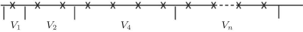 | Fig. 1. Diagrammatic sketch of one Josephson junction array. |
The Nb film is deposited with a sputtering power of 500 W, corresponding to a deposition rate of 0.75 nm/s. The Nb film with compressive stress of about 100 MPa and critical temperature of 9.1 K is obtained. The NbxSi1−x film is co-sputtered by using another Nb target and the Si target together, the Si sputtering power is 248 W and the Nb sputtering power is 37 W, which lead to a deposition rate of 0.17 nm/s. The thicknesses of the trilayer are 300 nm, 35 nm, and 200 nm, respectively.
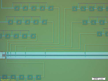
The sample is patterned by using photo lithography for all etching and liftoff processes. The top Nb layer and the NbxSi1−x barrier layer are etched to have steep edges by using reactive ion etching (RIE) and inductively-coupled-plasma (ICP) etching processes with a mixture gas of SF6 and C4F8.[10] A 400-nm thick SiO2 film is used as the insulating layer of the junction and it is deposited by using a plasma enhanced chemical vapour deposition (PECVD) system. RIE with ICP is also used for Nb base electrode etching using CF4 and O2 gas mixture and SiO2 etching using CHF3 and O2 gas mixture. An in-situ cleaning process by DC-biased rf etching is applied before depositing the 500-nm thick Nb wiring electrode, which enables a good contact between the upper Nb layer and the wiring electrode. For Nb wiring layer etching, only RIE is used with SF6. The resistance layer PdAu is deposited for microwave absorption by electron beam evaporation. Then the liftoff process for the PdAu film is performed. More details about the fabrication process have been provided in our previous paper.[11] Figure
 | Fig. 2. Part of the Josephson junction array chips. |
The sample is mounted onto a red cooper stage and connected to a printed circuit board by using aluminum silicide bonding wires. The stage is connected to the bottom of a probe stick which can be put into a helium Dewar. So the sample can be measured in the liquid helium at 4.2 K. Since the smallest voltage step generated by this sample is only 1 μV, a precise measurement system is necessary. A DC current source is used to sweep the sample by increasing the current step by step. An Agilent 34420A is used to measure the voltage across the sample. It is found that without shielding, the critical current and the voltage step are drifting all the time. When a lead shielding is used, the characteristics of the sample become stable.
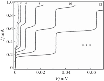
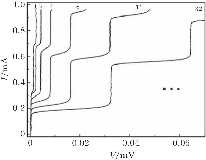
Figure
 | Fig. 3. The DC I–V characteristics for different numbers of Josephson junctions in series. The number of junctions is given in the figure. |
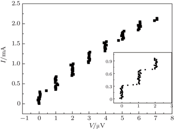
Although the characteristic voltage Vc is much larger than 1 μV, we also try to use the array at 483.59 MHz. For a single junction, it will develop constant voltage steps corresponding to integer times of one microvolt as shown in Fig.
 | Fig. 4. The I–V characteristics for a single Josephson junction driven by 483.59 MHz microwave. Insert is the detail of the first step, showing an over 200 μA flat region. |
 | Fig. 5. The I–V characteristics for different parts of the Josephson junction array driven by 483.59 MHz microwave. |
For different parts of the array, the I–V characteristics with microwave radiation are shown in Fig.
For microvolt applications, a Josephson junction array chip has been designed and fabricated. The DC and AC characteristics have been measured. The results demonstrate good uniform characteristics of the junctions. A 1 μV step with over 200 μA flat region has been observed. By selecting different parts of the array, it can output a quantum voltage from 1 μV to 256 μV. It is useful for potential applications, for example, calibrations of instruments working in the microvolt range or combining with PJVS to output more precisely AC voltage waveforms. In the future, we will adjust the barrier parameters of the junctions to obtain a wider voltage step of about 1 mA at several hundred MHz.
| 1 | |
| 2 | |
| 3 | |
| 4 | |
| 5 | |
| 6 | |
| 7 | |
| 8 | |
| 9 | |
| 10 | |
| 11 | |
| 12 |