


Electron transport in electrically biased inverse parabolic double-barrier structure
[Bati M1, 2, 3, †,  , Sakiroglu S1, Sokmen I1]
, Sakiroglu S1, Sokmen I1]
|
|


† Corresponding author. E-mail:
A theoretical study of resonant tunneling is carried out for an inverse parabolic double-barrier structure subjected to an external electric field. Tunneling transmission coefficient and density of states are analyzed by using the non-equilibrium Green’s function approach based on the finite difference method. It is found that the resonant peak of the transmission coefficient, being unity for a symmetrical case, reduces under the applied electric field and depends strongly on the variation of the structure parameters.
Resonant tunneling characteristics in resonant tunneling diodes (RTD) have become an attractive research area from both theoretical and technological points of view.[1] Survey of the electronic transport properties of nanoscale systems has a significant importance in the development of high-speed and high-frequency devices such as power memory cells, high speed logic and adders, diodes and quantum integrate circuits.[2] To clearly understand the dynamics characteristics of nanoscale devices, quantum transport models should be considered.[3] Wigner function method,[4] the kinetic Monte Carlo method,[5] the transfer matrix method (TMM),[6] and the non-equilibrium Green’s function (NEGF) method[7,8] are extensively used methods for modeling of transport in these devices.
Among the different quantum formalisms developed during the last decades,[9] non-equilibrium Green’s function method initiated by the works of Keldysh, Kadanoff, Baym, and Schwinger[7,8] stands as one of the most powerful and general approach. It provides a qualitative comprehension of quantum transport by allowing the inclusion of scattering mechanisms, contact and gate couplings. The NEGF method has been applied successfully to a great variety of systems ranging from phonon transport,[10–13] spin transport,[14–19] to electron dynamics in metals,[20–22] organic molecules and fullerenes,[23–27] and semiconductor nanostructures.[28–32] The main route in the application of NEGF formalism to finite structures[33–37] is division of the domain into the left contact, the right contact and the channel. The effect of contacts on a device is described by a self-energy quantity, which can be viewed as an effective potential or effective Hamiltonian. Self-energy can be derived by restricting the infinite domain Green’s function into a finite region.[36,37] In fact, this quantity is closely related to the artificial boundary conditions in the numerical solutions of NEGF.[38,39] Different numerical discretizations of the Hamiltonian of quantum device are possible, such as finite difference method (FDM) and finite element method (FEM), in which self-energy takes on different forms.[40]
Semiconductor diodes incorporating the double-barrier resonant structure are known as RTD. Resonant tunneling phenomenon allows the manufacturing of diodes with extremely high switching speeds (as high as THz region) and are therefore being studied in great detail.[9] Besides being technologically interesting, the RTD is also important as a simple test case for different formalisms and computational schemes. Owing to advances in nanofabrication technology, it has become possible to manufacture high-quality resonant tunneling structures with a wide variety of potential shapes such as rectangular, triangular, trapezoidal and parabolic.[41–44] Mostly in the simple model which offers an advantage for numerical calculation, the barriers are considered with rectangular form. References [45] and [46] reported the dependence of resonant tunneling characteristics on the structure parameters and external electric field in triangular double-barrier structures. Impressive progress in epitaxial growth techniques renders possible the realization of double barrier (well) structures composed of gradient and horizontal potentials by using both compositional grading and layer thickness variations. Reference [47] studied the tunability of the states of two coupled parabolic quantum wells whereas Shen and Rustgi[48] have also taken into account the effect of an electric field. Despite several works having been devoted to the search of rectangular double-barrier (RDB) structure and coupled parabolic quantum wells, to the best of our knowledge, no effort has been paid to the resonant tunneling characteristics of inverse parabolic double-barrier (IPDB) structure. The parabolic barrier is of particular importance in chemical and physical problems because it stands as a realistic representation of a real barrier, at least when tunneling involves only the upper part of the barrier. This is due to the fact that any curve with a finite radius of curvature can be approximated by a parabola over a limited range.[49] Therefore, in this paper, we address ourselves to survey the transmission probability in IPDB structure. The effects of the external electric field and the structural parameters are investigated in details. This type of barrier model is found suitable to parameterize nuclear fission barriers[50] and can constitute an example for the resonant tunneling diodes.
The outline of the rest of this paper is as follows. In Section 2, we present the model and methodology used throughout the work. Numerical results are given in Section 3 and finally Section 4 summarizes our conclusions.
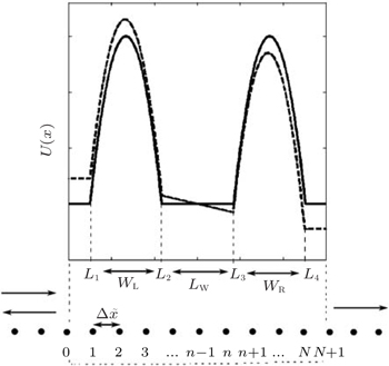
We consider an inverse parabolic double-barrier structure, whose well of width LW is located between two inverse parabolic barriers defined by widths WL and WR associated with the left and right barrier, respectively. As depicted in Fig.
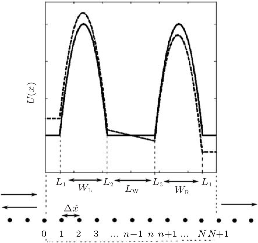 | Fig. 1. Schematic representation of the device considered in this work. The solid line represents the potential profile of symmetrical IPDB structure and dashed lines stands for case when the electric field is applied. |
To establish the non-equilibrium Green’s function formalism based on finite difference discretization, we describe one-dimensional Schrödinger equation for a device consisting of an active area connected to two semi-infinite contacts as follows:


Here we briefly overview the NEGF approach based on finite difference method (FDM-NEGF) to calculate transmission coefficient and density of states. The method inquires to find the retarded Green’s function of the system G. Assuming the device region is divided into N grid points with uniform spacing, Δx̃, finite difference discretization on the one-dimensional grid is applied to the dimensionless Schrödinger equation (Eq. (

The coupling of the device to the left and right contacts is taken into account by rewriting Eq. (

In addition, self-energy terms [
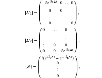


Finally, transmission coefficient T(Ẽ) can be computed as follows:

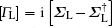


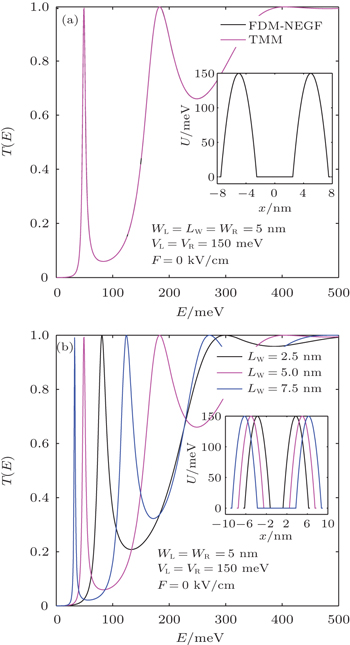
To study the transmission coefficient (T(E)) in inverse parabolic double-barrier structure, we assume the effective mass of the electron 0.067m0 (m0 is free-electron mass) to be constant through the system. In Fig.
 | Fig. 2. (a) Transmission coefficient of potentially symmetric IPDB as a function of electron energy calculated by using TMM and FDM-NEGF methods for constant LW = 5 nm. (b) Variation of the transmission coefficient with respect to well width. In both subfigures we use WL = WR = 5 nm, VL = VR = 150 meV. |
It is seen from the figure that the transmission coefficient exhibits resonant peaks and valleys. The first peak in transmission coefficient corresponds to the resonant tunneling associated with the fundamental quasi-bound state energy and is unity. Figure
In resonant tunneling structures, general symmetry plays a central role in the resonance while asymmetry causes reduction in the heights of the transmission peaks at resonance energies.[51] In the light of this knowledge, in Fig.
 | Fig. 3. Transmission coefficient as a function of electron energy calculated for two different (a) height asymmetries (VL = 100 meV and VL = 125 meV) and (b) thickness asymmetries (WL = 1 nm and WL = 2.5 nm). We set LW = WR = 5 nm and VR = 150 meV. |
Investigation of resonance conditions taking into account effect of an external electric field has a crucial role for realistic device designing.[53,54] The influence of an electric field turns up in a respect of breaking the symmetry of the resonant tunneling structure. Several works reported that the value of the transmission coefficient is reduced when an electric field is applied to symmetrical RDB structures and optimum transmission coefficient could be achieved in properly optimized asymmetrical structures. In this part of our work, we examine the dependence of the T(E) on the electric field as depicted in Fig.
 | Fig. 4. Dependence of the transmission coefficient on the varying values of the (a) electric field at VL = VR = 150 meV, and (b) height of the barriers at F = 30 kV/cm. In both subfigures we set WL = LW = WR = 5 nm. |
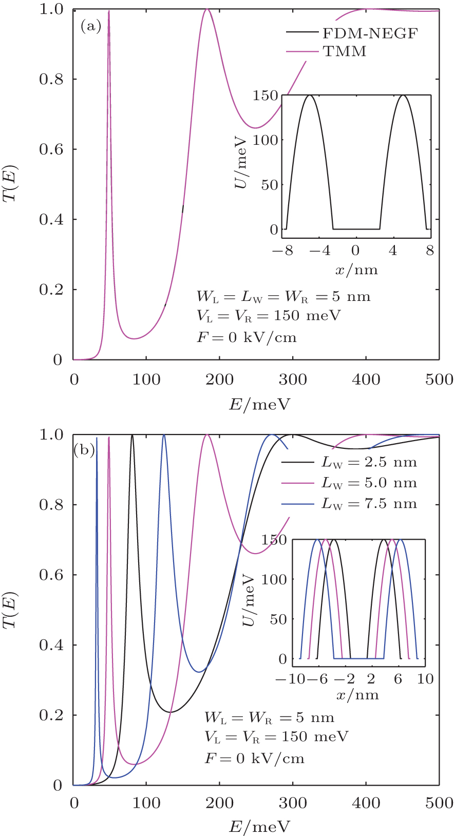
In order to expose the effect of structure parameters, considering the existence of external electric field (F = 30 kV/cm), in Fig.
 | Fig. 5. Dependence of the transmission coefficient calculated by FDM-NEGF on the varying values of (a) barrier widths at LW = 5 nm, and (b) well widths at WL = WR = 5 nm. In both subfigures we set VL = VR = 150 meV and electric field is chosen to be F = 30 kV/cm. |
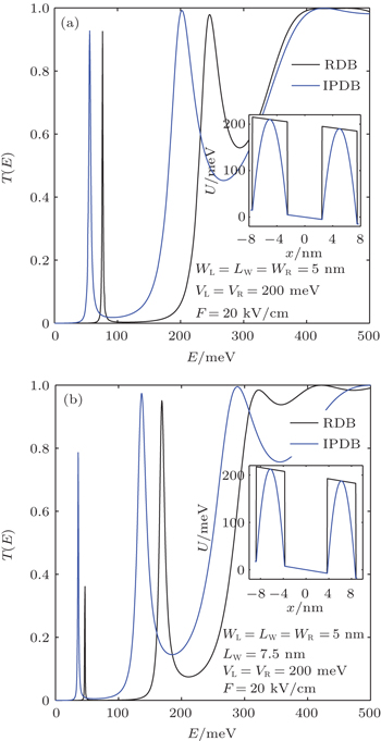
In the following part of the study, in order to illustrate the effect of the smoothness in the potential profile, we compare the results of transmission probability in IPDB structures with RDB given in Fig.
 | Fig. 6. Comparison of the transmission coefficient in the RDB and IPDB structures for two different values of well width (a) LW = 5 nm and (b) LW = 7.5 nm. Electric field of 20 kV/cm is taken and we chose WL = WR = 5 nm and VL = VR = 200 meV. |
From Fig.
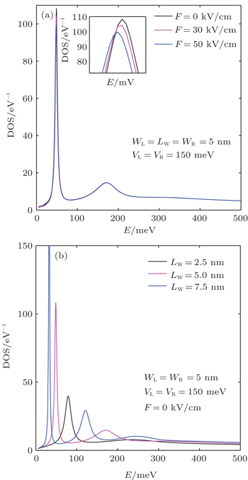
Finally, in Fig.
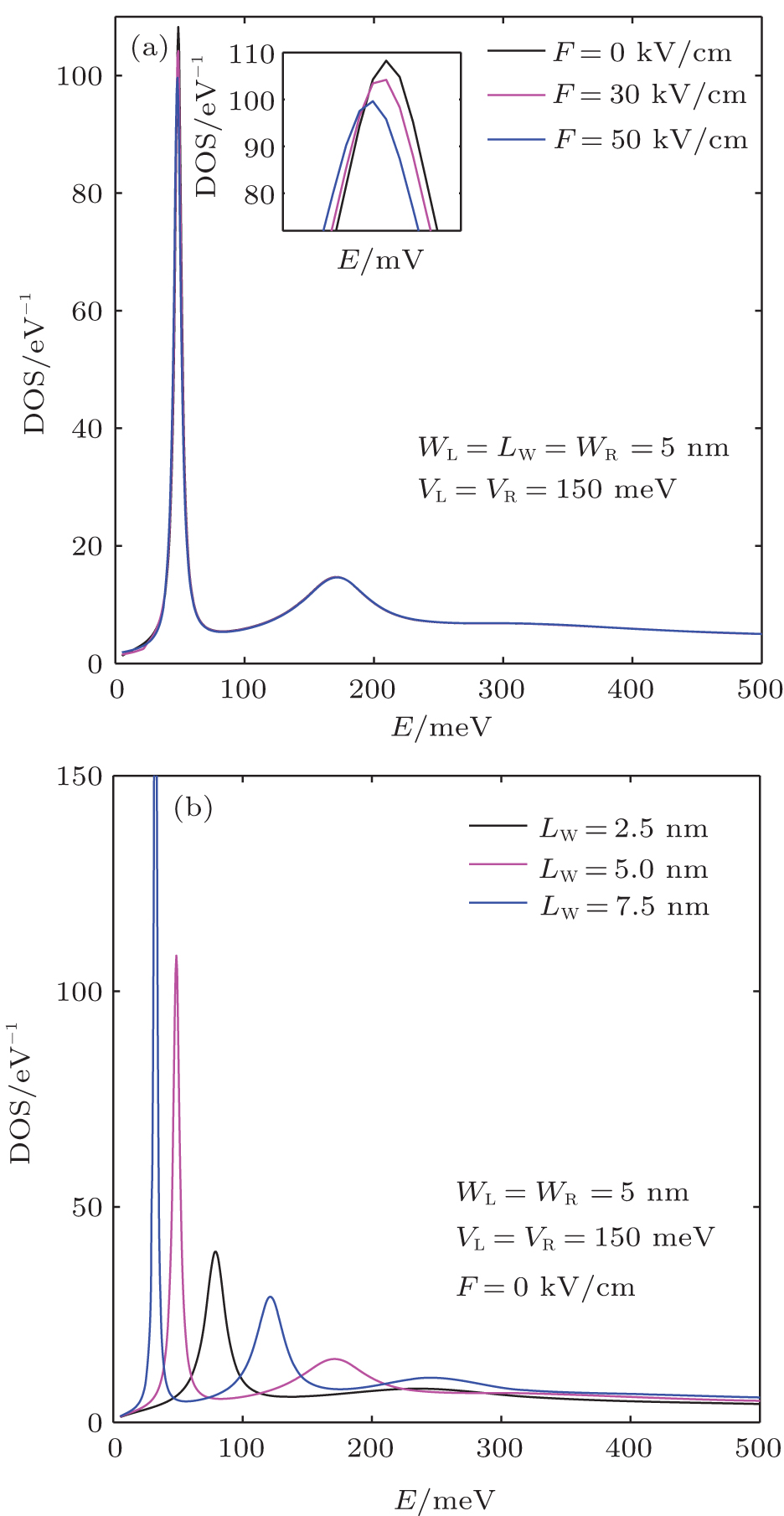 | Fig. 7. Calculated DOS as a function of energy for IPDB structure. (a) For varying electric fields for the same parameters as that in Fig. |
It is evident that, comparatively sharper and higher peak of DOS shifts to lower energy with the increment in electric field. Besides, as seen in the inset, small variation in the peak magnitude is observed. Dependence of DOS on the well width for zero-electric field is depicted in Fig.
In this paper, we investigate the electric field-induced ballistic transport in inverse parabolic double-barrier structure. The dependence of transmission coefficient on the well width, barrier height and width is analyzed. Numerical results for tunneling transmission probability show complete matching between finite difference method-based non-equilibrium Green’s function scheme and transfer matrix method. It was found that unity transmission observed in the absence of electric field for a symmetrical composition of barriers deteriorates when the asymmetrical case turns up. A distinctive feature of the resonant energy emerges for varying widths and heights of the potential barriers in the presence of electric field. The calculated results affirmed that the structure parameters of the system and external field affect strongly the resonant tunneling characteristics and thus can be controlled by these parameters. It is believed that the results could shed light on understanding of the transport properties of resonant tunneling devices.
| 1 | |
| 2 | |
| 3 | |
| 4 | |
| 5 | |
| 6 | |
| 7 | |
| 8 | |
| 9 | |
| 10 | |
| 11 | |
| 12 | |
| 13 | |
| 14 | |
| 15 | |
| 16 | |
| 17 | |
| 18 | |
| 19 | |
| 20 | |
| 21 | |
| 22 | |
| 23 | |
| 24 | |
| 25 | |
| 26 | |
| 27 | |
| 28 | |
| 29 | |
| 30 | |
| 31 | |
| 32 | |
| 33 | |
| 34 | |
| 35 | |
| 36 | |
| 37 | |
| 38 | |
| 39 | |
| 40 | |
| 41 | |
| 42 | |
| 43 | |
| 44 | |
| 45 | |
| 46 | |
| 47 | |
| 48 | |
| 49 | |
| 50 | |
| 51 | |
| 52 | |
| 53 | |
| 54 | |
| 55 |