Contact resistance asymmetry of amorphous indium–gallium–zinc–oxide thin-film transistors by scanning Kelvin probe microscopy
Wu Chen-Fei1, 2, Chen Yun-Feng1, 2, Lu Hai1, 2, †,  , Huang Xiao-Ming3, Ren Fang-Fang1, 2, Chen Dun-Jun1, 2, Zhang Rong1, 2, Zheng You-Dou1, 2
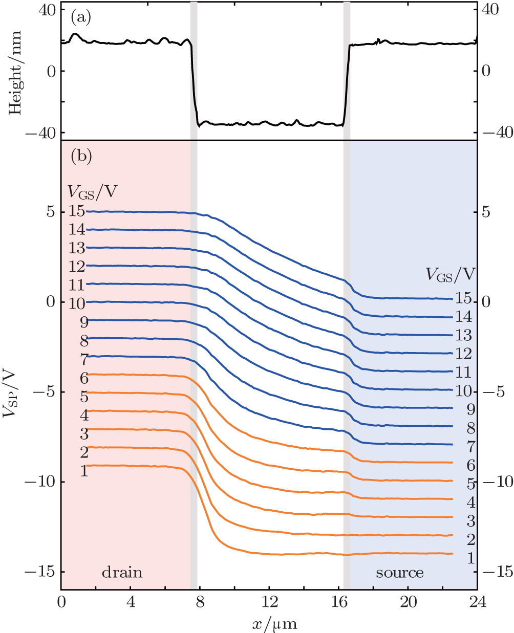
, Huang Xiao-Ming3, Ren Fang-Fang1, 2, Chen Dun-Jun1, 2, Zhang Rong1, 2, Zheng You-Dou1, 2 (a) Surface topography of the a-IGZO TFT along the channel length. (b) Surface potential profiles of the a-IGZO TFT with