


First-principles modeling hydrogenation of bilayered boron nitride
[Wang Jing, Zhang Peng, Duan Xiang-Mei†,  ]
]
]
 |


† Corresponding author. E-mail:
Project supported by the National Natural Science Foundation of China (Grant No. 11574167).
We have investigated the structural and electronic characteristics of hydrogenated boron-nitride bilayer (H–BNBN–H) using first-principles calculations. The results show that hydrogenation can significantly reduce the energy gap of the BN–BN into the visible-light region. Interestingly, the electric field induced by the interface dipoles helps to promote the formation of well-separated electron–hole pairs, as demonstrated by the charge distribution of the VBM and CBM. Moreover, the applied bias voltage on the vertical direction of the bilayer could modulate the band gap, resulting in transition from semiconductor to metal. We conclude that H–BNBN–H could improve the solar energy conversion efficiency, which may provide a new way for tuning the electronic devices to meet different environments and demands.
Energy is important which guarantees sustainable economic and social development. Nowadays, increasing energy and environmental problems lead to severe challenges for the survival of mankind. From a long-term perspective, solar energy is the only inexhaustible resource to meet the demand. Stimulated by the pioneering work of Fujishima and Honda,[1] which has proved that the photoelectrochemical (PEC) technique can generate hydrogen via water splitting, many efforts have been devoted to search for new photocatalysts that can readily take advantage of abundant sunlight energy to split water into hydrogen. Semiconductor photocatalysis can not only convert solar energy into chemical energy, but also directly degrade and mineralize organic pollutants, which solves the energy shortage and environmental pollution problems, thus showing great potential in artificial photosynthesis.[1–4] Still, most of the photocatalysts are facing the following difficulties: firstly, the band gap is too wide to absorb sunlight efficiently, for instance, titania can only respond to ultraviolet light, which is rarely part of the visible light region;[5–7] secondly, the electric potentials of valence band maximum (VBM) and conduction band minimum (CBM) are very hard to simultaneously meet the needs of reduction and oxidation potentials of water splitting; thirdly, the photo-produced electron–hole pair can easily recombine, which would decrease the catalytic efficiency;[8] lastly, photocatalysts which absorb visible light are not stable during the reaction process, for example, the photo corrosion occurs in CdS.[9] On the whole, both strong light absorption and suitable redox potential are prerequisites for photocatalytic reaction. Recently, 2D layered materials, such as g-C3N4,[10–13] graphene/TiO2,[14,15] g-C3N4/MoS2,[16] and so on, have attractive intensive research interests due to their visible-light-active photo-voltalic properties. From a theoretical point of view, it is needed to further explore new photocatalysts with visible light efficiency, high quantum efficiency, and high stability.
Based on first-principles calculations, Li et al.[17] proposed a novel reaction mechanism for water splitting, and proved that, in the near-infrared light region, hydrogen can be produced on a hexagonal boron-nitride (h-BN) bilayer saturated with H and F atoms on each surface. To obtain high optical absorption and high carrier mobility, the concentration and distribution of H and F must be strictly controlled, which may be difficult to achieve in the experiment. Hydrogenation and electric field are well used to tailor the electronic structures of the semiconductors.[11,18] In this paper, we systemically study the geometric and electronic characteristics of h-BN bilayer heterostructure subjected to hydrogenation. We find that the junction has a moderate direct band gap (1.30 eV), and can effectively use the visible light. On the other hand, we also note that the electronic properties of the material can be easily controlled by the external electric field perpendicular to the bilayer, which may provide a new way for tuning the electronic devices to meet different environments and demands. It is intriguing to see that the material can correspondingly switch from semiconductor to conductor.
Our first-principles calculations are based on density functional theory (DFT) with generalized gradient approximation (GGA)[19] for the exchange–correlation potential and Perdew–Burke–Ernzerholf (PBE) functional[19] for the GGA as implemented in the Vienna ab initio simulation package (VASP).[20] The interaction between the core and valence electrons is described using the frozen-core projected augmented wave (PAW) approach.[21,22] The dipole correction is applied to compensate the dipole interaction in the direction perpendicular to the plane. We apply periodic boundary conditions with a vacuum space of 30 Å along the z direction in order to avoid the interaction of neighboring junctions. The cutoff energy for the plane-wave basis is set to be 400 eV. Geometry optimizations are carried out until the convergence criterion for the energy (< 10−6 eV) is met and the forces on all the atoms are less than 0.01 eV/Å. A Monkhorst–Pack[23] k-mesh of 7×7×1 is adopted for optimization, while 15×15×1 is used for the self-consistent energy calculations. Both the lattice constant and the positions of all atoms are allowed to relax using the conjugated gradient method without any symmetric constraints. Since the GGA approach usually underestimates the band gap of a semiconductor, to obtain relatively accurate electronic structures and optical properties, we perform Heyd–Scuseria–Ernzerhof 2006 (HSE06)[24] calculation with the total exchange potential containing 20% of the Hartree–Fock exchange potential. We utilize the imaginary part of the frequency dependent dielectric function to evaluate the optical properties.
The stability of the nanostructures can be defined through the binding energy, which is obtained from the relation

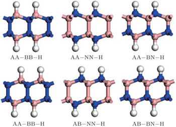
We consider five stacking constructions for BN bilayers, and confirm that the AB stacking structure, with B or N atom sited above the center of the other BN layer, is the lowest in energy among the structures, which agrees well with the previous theoretical results.[25] Considering that the stacking order of the hydrogenated bilayer BN may be affected by the saturated atoms, we check six adsorption sites for hydrogen (see Fig.
 | Fig. 1. Six possible configurations for H saturated on BN bilayers. The blue, pink, and white spheres represent N, B, and H atoms, respectively. |
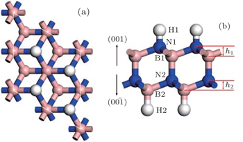
 | Fig. 2. (a) Top view and (b) side view of the configuration of H–BNBN–H. The blue, pink, and white spheres represent N, B, and H atoms, respectively. |
The optimized structure of H–BNBN–H is shown in Fig.
 | Fig. 3. (a) The calculated formation reaction pathway of H–BNBN–H from the combination of two functionalized single layers H–BN and BN–H. (b) Band structure of H–BNBN–H. The black solid and red dashed lines represent the GGA and the hybrid HSE06 results, respectively. |
Since the junction is asymmetric (shown in Fig.

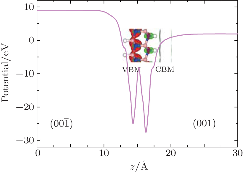 | Fig. 4. Plane-averaged electrostatic potentials along the z direction and the VBM (in red) and CBM (in green) distributions of H–BNBN–H. The calculated electrostatic potential difference of the (00 |
We perform the Bader analysis[29] of the charge density, and list the results in Table
| Table 1. The Bader charge analysis of the optimized H–BNBN–H, comparing to the separated AB stacking BN bilayer and H. . |
The photocatalytic conditions of PEC water splitting are as follows: the oxidation potential on the (00

The spontaneous PEC water-splitting process needs to utilize both the reduction and powers of H–BNBN–H. The oxidation power is measured by the VBM, the lower the VBM energy, the stronger the oxidizing power. The reducing power is evaluated by the CBM, i.e., the closer the CBM to the vacuum level, the stronger the reducing power. We examine the locations of VBM and CBM with respect to the redox potentials of water splitting, and find that the reaction conditions are well satisfied. Figure
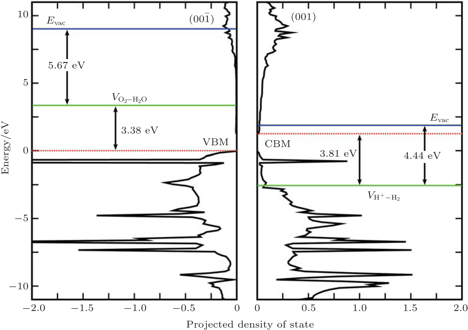 | Fig. 5. Energy diagram of H–BNBN–H. The vacuum level (Evac), redox potentials of water (VO2−H2O, VH+−H2), VBM, and CBM are denoted by labeled lines. |
The optical properties are calculated by the frequency dependent dielectric function ε(ω) = ε1(ω) + iε2 (ω), which is mainly a function of the electronic structure. The imaginary part of the dielectric function, ε2(ω), can be calculated by a summation over empty states using the equation[31]

 | Fig. 6. The energy-dependent imaginary part of the dielectric function ε2(ω) with the polarization vector parallel and perpendicular to the z axis, where the energy range of visible light is marked by vertical short blue lines. |
Generally, the dipole-induced electric field could increase (decrease) the energy of the VBM (CBM) and lead to a relatively small band gap of the junction, it is natural to see whether H–BNBN–H can be tuned by an external electric field. We apply a perpendicular electric field to the junction, and present the response of the material in Fig.
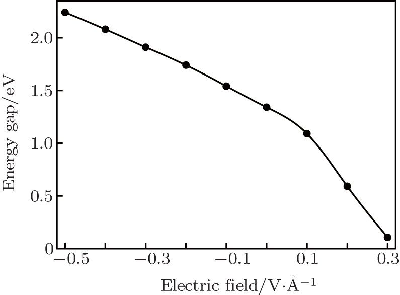 | Fig. 7. The calucated energy gap of H–BNBN–H as a function of the external electric field. |
Based on the first-principles calculation, we have carefully studied the electronic structures and optical properties of the fully hydrogenated bilayered boron nitride, and analyzed the character of the redox reaction. The moderate dipole at the interface plays an important role in the electronic structures of the system. Moreover, as a photocatalysis semiconductor, H–BNBN–H meets the requirement of the water splitting reaction, and the optical absorption edges cover the whole visible light region. The hydrogenated junction is sensitive to the external electric field. In view of the recent progress, our results provide a practical scheme for the photovoltaic materials.
| 1 | |
| 2 | |
| 3 | |
| 4 | |
| 5 | |
| 6 | |
| 7 | |
| 8 | |
| 9 | |
| 10 | |
| 11 | |
| 12 | |
| 13 | |
| 14 | |
| 15 | |
| 16 | |
| 17 | |
| 18 | |
| 19 | |
| 20 | |
| 21 | |
| 22 | |
| 23 | |
| 24 | |
| 25 | |
| 26 | |
| 27 | |
| 28 | |
| 29 | |
| 30 | |
| 31 | |
| 32 | |
| 33 | |
| 34 | |
| 35 | |
| 36 |