


Optical bistability and multistability in a defect slab doped by GaAs/AlGaAs multiple quantum wells
[Hossein Asadpour Seyyed†,  , Solookinejad G, Panahi M, Ahmadi Sangachin E]
, Solookinejad G, Panahi M, Ahmadi Sangachin E]
 |


† Corresponding author. E-mail:
We proposed a new model for controlling the optical bistability (OB) and optical multistability (OM) in a defect slab doped with four-level GaAs/AlGaAs multiple quantum wells with 15 periods of 17.5 nm GaAs wells and 15-nm Al0.3 Ga0.7As barriers. The effects of biexciton energy renormalization, exciton spin relaxation, and thickness of the slab on the OB and OM properties of the defect slab were theoretically investigated. We found that the transition from OB to OM or vice versa is possible by adjusting the controllable parameters in a lab. Moreover, the transmission, reflection, and absorption properties of the weak probe light through the slab were also discussed in detail.
In the last few decades, the theoretical and experimental studies related to quantum coherence and quantum interference based phenomena, such as electromagnetically induced transparency (EIT),[1–3] lasing without inversion,[4] giant Kerr nonlinearity,[5–7] four-wave mixing,[8,9] and so on,[10–17] have been carried out in multi-level atomic systems. In quantum and nonlinear optics, optical bistability (OB) and optical multistability (OM) due to their important applications in quantum memories, all-optical switching, and logic circuits[18] have been discussed by several groups.[19–32] It is worth pointing out that the general method for analyzing the optical bistability is based on the feedback mechanism in the unidirectional ring cavity confined with atomic samples.[19–32] Joshi et al.[19] discussed experimentally the optical bistable behavior in an optical ring cavity filled with a collection of three-level Λ-type rubidium atoms interacting with two collinearly propagating laser beams. They found that the bistability is very sensitive to the induced atomic coherence in this system and, thus, can be easily controlled by changing the intensity and the frequency detuning of the coupling field. Then, many models have been proposed for analyzing the OB and OM in multi-level atomic systems via laser coherent fields,[20–22] spontaneously generated coherence (SGC),[23–26] the injection of squeezed light,[27] the atomic cooperation parameter,[28] and so on. For example, Xiao and Kim[22] investigated the OB in an optical system which consists of a four-level atomic system with a microwave drive field and an optical cavity. They found that the OB can be accomplished by adjusting different physical parameters in both steady and transient processes. They showed that due to the existence of the microwave drive field, the optical bistability can also be obtained even under the weak coherent coupling field condition. The quantum interference effect from incoherent pumping field and spontaneous emission on OB properties in a V-type three-level atomic system confined in a unidirectional ring cavity was investigated in Ref. [29]. It was found that the OB can be controlled by the rate of the incoherent pumping field and by the interference mechanism arising from the spontaneous emission and the incoherent pumping field. Polarized control of OB in a four-level tripod atomic system has been discussed in Ref. [30]. It was demonstrated that the OB behaviors can be controlled efficiently by adjusting the system parameters and the relative phase of the applied fields. Wang et al.[31] proposed a model for manipulating the OB in an open three-level Λ-type atomic system confined in a unidirectional ring cavity. They found that the OB behaviors can be controlled by the incoherent pumping rate and the spontaneously generated coherence.
It should be noted that quantum coherence and quantum interference can lead to manipulation of nonlinear quantum optical phenomena in the semiconductor quantum wells (SQWs) and quantum dots (SQDs).[33–46] The OB behaviors of a three-level quantum well nanostructure confined in a unidirectional ring cavity have been studied.[33] In another study,[34] the absorptive-dispersive OB behavior via tunable Fano-type interference based on the intersubband transitions in asymmetric double quantum wells driven coherently by a probe laser field by means of a unidirectional ring cavity has been analyzed. It was shown that the OB can be controlled efficiently by tuning the energy splitting of the two excited states (the coupling strength of the tunnelling), the Fano-type interference, and the frequency detuning. The influence of the electronic cooperation parameter on the OB behavior has also been discussed. In another study, Li[35] analyzed the OB properties of an asymmetric coupled-quantum well based on the intersubband transitions driven coherently by a probe laser field and a control laser field by means of a unidirectional ring cavity. It was demonstrated that the OB can be controlled by tuning the energy splitting between two tunnel-coupled electronic levels, the intensity of the control field, and the frequency detuning of the probe and the control fields. The SQW and SQD due to their wide potential applications in optoelectronics and solid-state quantum information science have been analyzed by many research groups.[47–49] The large electric dipole moments due to the small effective electron mass, the great flexibilities in device design by choosing the materials and the structure dimensions, and the high nonlinear optical coefficients make these structures have advantages over the atomic systems. Very recently, Yang et al.[47] discovered control of the Goos–Hänchen (GH) shift of a mid-infrared probe beam in a cavity consisting of an asymmetric double quantum well nanostructure. They obtained the maximum negative and positive GH shifts in transmitted and reflected light when the quantum interference from electron tunneling was considered.
Unlike the general method for achieving the optical bistability, we propose a new model for analyzing the optical bistability in a dielectric medium with a defect layer of multiple quantum well nanostructure. By using the transform matrix method, we calculate the transmission and reflection coefficients of the incident probe light to the defect slab, and then discuss the OB behaviors of the transmitted light through the defect slab. To the best of our knowledge, there are no theoretical or experimental works related to OB and OM in a slab with a defect layer of multiple quantum well nanostructure. We will discuss the effects of the biexciton energy renormalization, the exciton spin relaxation, and the thickness of the slab medium on the OB and OM behaviors of the incident light. Here, the structure of multiple quantum wells is based on that in Ref. [50]; however, our work is drastically different from that work. First and foremost is that we are interest in showing the controllability of OB and OM in a defect slab. Second, the thickness of the slab is considered as a new parameter for controlling the OB and OM behaviors of the weak probe light.
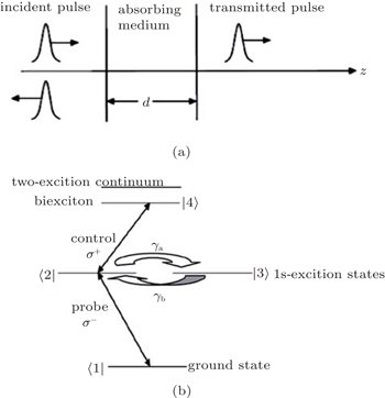
In the following, the pulse propagation in a slab and the structure of the doped MQWs in the defect layer of the slab will be discussed. It is assumed that the incident pulse normally propagates through the dielectric medium along the z direction (Fig.


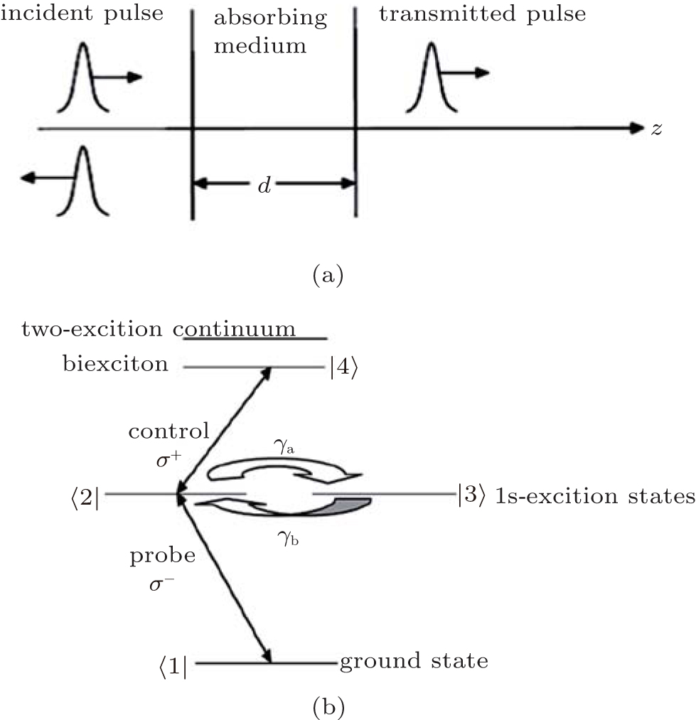 | Fig. 1. (a) Schematic of the weakly absorbing dielectric slab. (b) Schematic energy-level diagram of the GaAs multiple quantum wells. |
We consider the MQWs as a dispersive layer in the dielectric slab and study its level structure. The energy levels of the GaAs MQWs form a four-level system where a control beam drives the transition |2〉 → |3〉 while a weak probe beam couples to the transition |1〉 → |2〉 (Fig.


To investigate the OB behavior of the slab, one can use the relationship between the incident intensity Uin and the transmitted intensity Ut

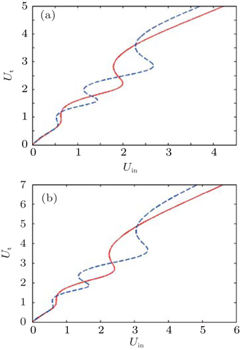
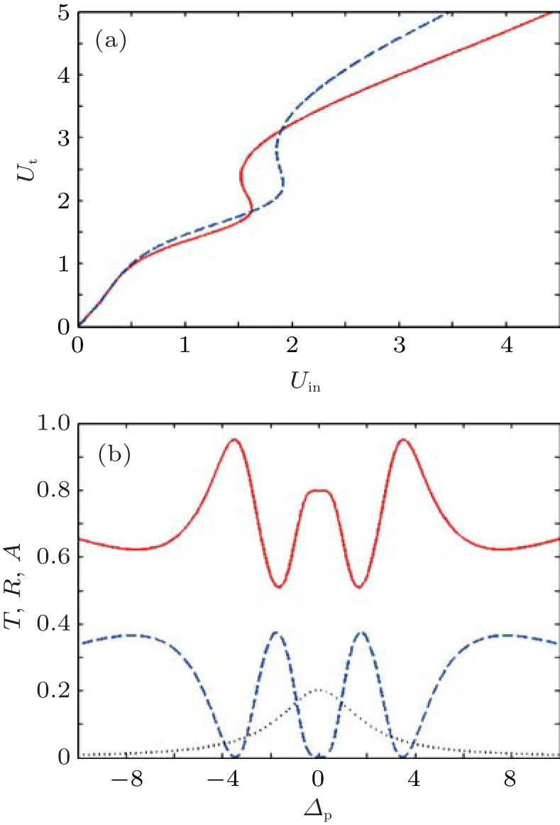
 | Fig. 2. The transmitted intensity of the probe field Ut versus the incident intensity Uin for different coupling fields. The solid line corresponds to Ωc = 0.2, dashed line corresponds to Ωc = 2, and dotted line corresponds to Ωc = 5. The other selected parameters used are ɛb = 4, λ0 = 1.55 μm, Δp = 0.5, Δc = 0, γi = 1, γa = γb = 0, and β = 0. |
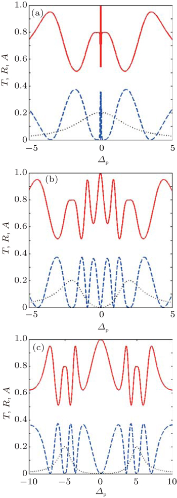
 | Fig. 3. Transmission (solid), reflection (dashed), and absorption (dotted) properties of the incident light versus probe detuning for (a) Ωc = 0.2, (b) Ωc = 2, and (c) Ωc = 5. The selected parameters are the same as those in Fig. |
 | Fig. 4. (a) The transmitted intensity of the probe field Ut versus the incident intensity Uin for γb = γa = 0 (solid) and γb = γa = 1 (dashed). (b) Transmission (solid), reflection (dashed), and absorption (dotted) properties of the incident light versus detuning of the probe light in the presence of exciton spin relaxation. The used parameters are the same as those in Fig. 2 and Ωc = 0.2. |
 | Fig. 5. The transmitted intensity of the probe field Ut versus the incident intensity Uin for (a) m = 100 and (b) m = 150. The selected parameters are the same as those in Fig. |
 | Fig. 6. (a) The transmitted intensity of the probe field Ut versus the incident intensity Uin for β = 0, (solid) and β = 1 (dashed). (b) Transmission (solid), reflection (dashed) and absorption (dotted) properties of the incident light versus detuning of the probe light in the absence of exciton spin relaxation. The used parameters are the same as those in Fig. |
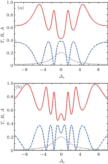
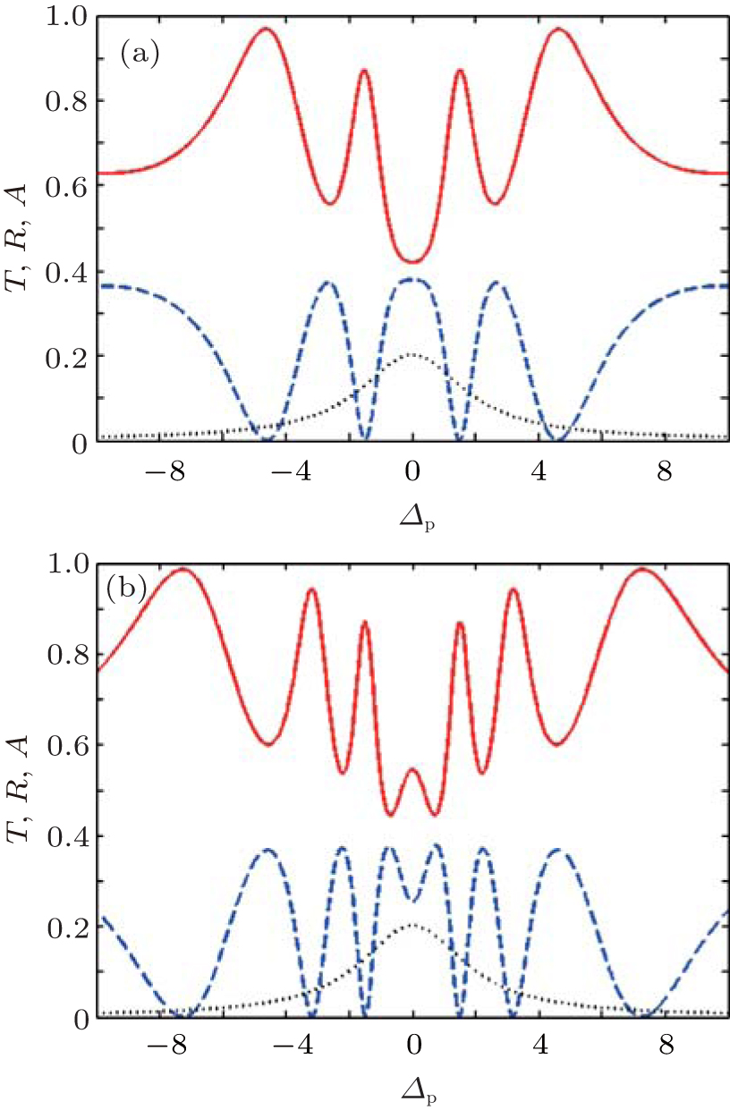 | Fig. 7. Transmission (solid), reflection (dashed), and absorption (dotted) properties of the incident light versus detuning of the probe light for (a) m = 100 and (b) m = 150. The selected parameters are γb = γa = 1, β = 1, Ωc = 2 and the others are the same as those in Fig. |
The effect of coherent coupling on the OB behavior of the probe field is investigated in Fig.
In Fig.
In the next section, we study the effect of the thickness of the slab on the OB behavior of the probe field. The OB behavior of the probe field for different thicknesses in the absence and presence of the exciton spin relaxation is displayed in Fig.
In the following, we analyze the effect of the biexciton energy renormalization on the OB behavior of the probe field in the slab. The effects of the biexciton energy renormalization can be simulated by replacing ωb with 
Finally, we plot the transmission (solid), reflection (dashed), and absorption (dotted) of the probe light for m = 100 and m = 150 in the presence of the exciton spin relaxation and biexciton binding energy in Fig.
We investigated the OB and OM behaviors of the four-level multiple quantum well nanostructure inside a dielectric slab. We found that by adjusting some controllable parameters such as the intensity of the coupling field, the exciton spin relaxation, the biexciton binding energy, and the thickness of the slab, the intensity threshold of OB can be controlled, and for some parameters, the switching between OB and OM can occur. Moreover, the transmission, reflection, and absorption of the weak probe light through the cavity have been discussed. We found that the switching from subluminal to superluminal or vice versa can be obtained for the reflected and transmitted light from the slab.
| 1 | |
| 2 | |
| 3 | |
| 4 | |
| 5 | |
| 6 | |
| 7 | |
| 8 | |
| 9 | |
| 10 | |
| 11 | |
| 12 | |
| 13 | |
| 14 | |
| 15 | |
| 16 | |
| 17 | |
| 18 | |
| 19 | |
| 20 | |
| 21 | |
| 22 | |
| 23 | |
| 24 | |
| 25 | |
| 26 | |
| 27 | |
| 28 | |
| 29 | |
| 30 | |
| 31 | |
| 32 | |
| 33 | |
| 34 | |
| 35 | |
| 36 | |
| 37 | |
| 38 | |
| 39 | |
| 40 | |
| 41 | |
| 42 | |
| 43 | |
| 44 | |
| 45 | |
| 46 | |
| 47 | |
| 48 | |
| 49 | |
| 50 | |
| 51 | |
| 52 | |
| 53 | |
| 54 | |
| 55 | |
| 56 |