Yu Yue-Yang, Sun Xiao-Qiang, Ji Lan-Ting, He Guo-Bing, Wang Xi-Bin, Yi Yun-Ji, Chen Chang-Ming, Wang Fei, Zhang Da-Ming. The 650-nm variable optical attenuator based on polymer/silica hybrid waveguide. Chinese Physics B, 2016, 25(5): 054101
Permissions
The 650-nm variable optical attenuator based on polymer/silica hybrid waveguide
Yu Yue-Yang1, Sun Xiao-Qiang1, 2, †, , Ji Lan-Ting1, He Guo-Bing1, Wang Xi-Bin1, 2, Yi Yun-Ji1, 2, Chen Chang-Ming1, 2, Wang Fei1, 2, Zhang Da-Ming1, 2
State Key Laboratory on Integrated Optoelectronics, College of Electronic Science & Engineering, Jilin University, Changchun 130012, China
Jilin Provincial Engineering Laboratory on Polymer Planar Lightwave Circuit, Changchun 130012, China
† Corresponding author. E-mail: sunxq@jlu.edu.cn
Project supported by the National Natural Science Foundation of China (Grant Nos. 61205032, 61475061, 61405070, 61177027, 61275033, and 61261130586) and the Science and Technology Development Plan of Jilin Province, China (Grant No. 20140519006JH).
Abstract
Abstract
Visible light variable optical attenuators (VOA) are essential devices in the application of channel power regulation and equalization in wavelength-division multiplexing cross-connect nodes in plastic optical fiber (POF) transmission systems. In this paper, a polymer/silica hybrid waveguide thermo–optic attenuator based on multimode interference (MMI) coupler is designed and fabricated to operate at 650 nm. The single-mode transmission condition, MMI coupler, and transition taper dimensions are optimized through the beam propagation method. Thermal analysis based on material properties provides the optimized heater placement angle. The fabricated VOA presents an attenuation of 26.5 dB with a 21-mW electrical input power at 650 nm. The rise time and fall time are 51.99 and 192 μs, respectively. The time–stability measurement results prove its working reliability.
In the near future, high data rate networks over Gb/s are urgently needed for the application of multimedia technology in automobiles, automation, and at home in a large scale.[1] Compared with single-mode glass optical fiber that has been widely used in trunk lines for long-distance communications, polymethyl methacrylate (PMMA) polymer optical fiber or plastic optical fiber (POF) with a large core diameter and step-index (SI) profile has merits of low-cost, robustness to mechanical stress and immunity to electromagnetic interference, which make it a good candidate for home internet connections and automotive applications.[2,3] Recently, wavelength-division multiplexing (WDM) technology together with the progress of laser diodes and optimized receiver fabrication, became an effective way to increase the capacity of the visible light transmission in POF systems.[4–6] In addition, the signal amplification device with a gain of 14 dB at 650 nm has also been reported.[7] All these works provided good potentials of WDM data transmission for POF systems.
Variable optical attenuators (VOA) are essential devices in applications of gain control of optical amplifiers, channel power regulation and equalization in WDM cross-connect nodes and transmission systems.[8] Characteristics of fast response, wide attenuation range, and low insertion loss are crucial to the performance of VOA. Different approaches have been reported to implement a VOA.[9–12] Although many of them can provide desirable performances and reliability, polymer-based waveguide VOA offers a specific advantage in providing good compatibility with POF system. In addition, the polymer has a thermo–optic coefficient that is one order of magnitude larger than that of inorganic materials, such as silica.[8] Low-cost, easy fabrication, good optical and mechanical properties, and being compatible with different substrates allow the low-cost, large-scale integration of polymer VOA with a wide range of photonics components on a single chip.[13] TO controlled whole polymer VOA can be implemented by bent waveguide,[14] straight channel,[15] or interference coupler structures.[16] However, they either suffers precise dimension control and environment requirement, or long response time induced performance declining.
In this work, a multi-mode interference (MMI) coupler in the form of polymer/silica hybrid waveguide structure is proposed. Compared with whole polymer VOAs,[14–16] the adoption of silica with a high thermal conductivity as bottom cladding can overcome the deficiency of low thermal diffusion of polymer bottom-cladding, which is favorable to accelerating the relaxation of heat in the waveguide and improving time response performance. The adoption of MMI coupler improves the fabrication tolerance of dimension departures from the design ones. Besides, the polymer SU-8 cannot only provide a low optical absorption at 650 nm, but also a high TO coefficient that is good to decrease the absorption loss and power consumption. Here, waveguide dimensions are optimized by beam propagation method (BPM). Device performances of attenuation, power consumption, temporal response, as well as time stability are confirmed according to the applied voltage control.
2. Design and optimization
The proposed VOA consists of a pair of input/output single-mode waveguides connected to the tapered transition sections, a multimode waveguide coupler, and an electrode heater that is aligned at an angle of α to the MMI coupler above the upper-cladding, as shown in Fig. 1. The light coupled adiabatically from the single-mode input waveguide to the MMI section. When the electrical power is applied to the heater, the temperature gradients inside polymers will lead to a decrement of effective index of higher-order modes in the MMI region due to the thermo–optic effect. As a result, the light under the heater will be partially reflected at an angle of 2α with respect to the horizontal axis. If α is larger than the fundamental mode of the MMI coupler, the reflected light is supposed to be coupled back into higher-order modes, which will be filtered out ultimately by the output tapered region and the single-mode output waveguide. Deep attenuation can be realized by applying higher driving power, which will result in more light reflection.
Fig. 1. Schematic diagram of (a) cross-sectional view, and (b) top view of designed 650-nm optical attenuator.
2.1. Single-mode waveguide
Multiple-layer waveguide configurations, including the thickness, shape, and refractive indices of polymers, need to be tailored to fulfill single-mode propagation confinement. In this paper, the designed attenuator based on polymer/silica waveguide was supported by a silicon wafer, which facilitates heat flow. Poly(methyl-methacrylate-glycidly-methacrylate) (P(MMA–GMA)) synthesized by ourselves and commercial polymer SU-8 were used as the upper-cladding and core material, respectively, due to their stable chemical properties.[17,18] A thin silica layer on the silicon substrate was chosen to be the bottom-cladding to quicken the response. To enhance the thermal field modulation, the upper-cladding between the metal heater and core layer was chosen to be 2 μm, which was thick enough to restrain the metal induced optical loss.
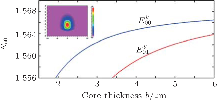
A rib waveguide architecture with desired mode shape was supposed to be used in this design. The relationship between the core thickness b and the effective refractive index Neff of the rib waveguide at a wavelength of 650 nm based on the effective index method (EIM) is shown in Fig. 2, where the waveguide width a is equal to b, the rib height h = 0.8b, the refractive indices n1 of SU-8 and n2 of P(MMA–GMA) materials were measured to be 1.568 and 1.51, respectively. Since the maximum thickness of SU-8 layer is determined by the condition in which mode began to exist or cut-in, therefore, b is supposed to be within 3 μm to realize single-mode propagation of mode in the rib waveguide. The fundamental optical mode profile calculated by the beam propagation method (BPM) is shown in the inset of Fig. 2. It can be seen that the optical power is well confined in the SU-8 core layer, which is favorable to restrict the radiation-induced optical loss.
Fig. 2. Relationship between the core thickness b and effective refractive index Neff of the rib waveguide with a = b and h = 0.8b. The inset shows the fundamental optical mode profile calculated by the beam propagation method.
2.2. MMI coupler
The MMI coupler plays a key role in the operation of the attenuator. The working principle of MMI coupler is based on the self-imaging effect that an interference pattern consisting of a single or multi-fold reproduction of the input field appears periodically when sufficient modes are excited along the MMI region. The input power can be coupled to the output single-mode waveguide with low insertion loss through the propagation of higher-order modes besides the fundamental mode.[19,20] It is well known from the MMI self-imaging theory that N-fold images of the input field are obtained at distances
where p ≥ 0 and N ≥ 1 are integers that have no common divisor, Lπ, known as the beat length between two lowest-order modes of light, can be described as
where β0 and β1 are propagation constants of the fundamental and the first-order lateral modes, respectively, λ0 is the free-space wavelength, n is the effective refractive index, and We is the effective width of the multimode waveguide. Due to the symmetry of the input field at coupler entrance, only even eigenmodes can be generated when a single-mode input waveguide is centrally positioned to the MMI section.[21] When n = 1.542 and We = Wmmi = 24 μm, Lπ is calculated to be 1822 μm. Hence, the mirrored single image of the input field will emerge at L = 1366 μm. To enhance the mode interference, an MMI waveguide length of 3L = 4098 μm can be adopted.
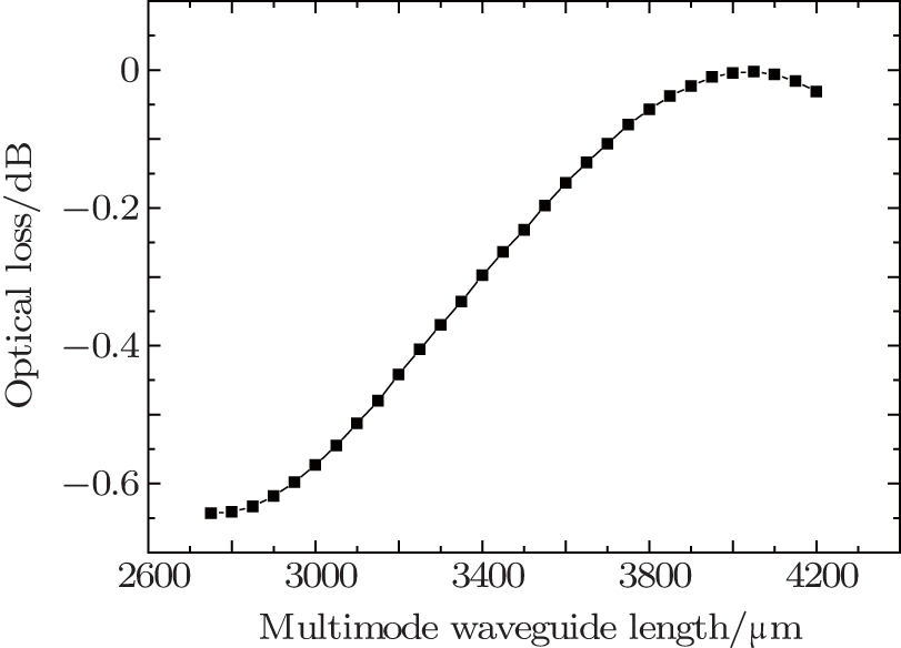
However, these equations and conclusions are based on the assumption that the core and cladding materials have a high refractive index contrast, under which conditions the optical penetration depth is very small so that the effective width of the multimode waveguide We can be considered to be the geometrical dimension Wmmi. In this design, the refractive index of the core material SU-8 is 1.568, while cladding materials of P(MMA–GMA) and SiO2 are 1.51 and 1.46, respectively. This low refractive index contrast will inevitably lead to a deeper penetration of mode field into claddings, which results in errors between We and Wmmi. As a result, the calculated Lπ based on We = Wmmi does not precisely accord with the practical conditions. Therefore, BPM method is employed for the optimization of MMI coupler dimensions. Mode coupling and power propagation damping in the MMI region will also happen. Therefore, the length of MMI coupler needs to be optimized with defined width and architecture. As shown in Fig. 3, when the calculated width We is 24 μm, an MMI waveguide with a length of L = 4050 μm is more favorable to realize low insertion loss.
Fig. 3. Optical insertion loss with the variation of MMI coupler length.
2.3. Tapered transition waveguide
The transition waveguide should ensure that the first-order mode could propagate adiabatically with no transforming to higher-order or radiated modes, which means that the fundamental mode should maintain most power after propagating a certain distance. A general consensus on tapered waveguides is that if a taper is made long enough, and has a gradual enough taper slope, the loss will be very low. Therefore, the conversion loss from the input single-mode waveguide and MMI waveguide would be minimized by a proper design of the transition waveguide structure. The mode adapter with a gradual tapering shape of parabolic, linear, or exponential tapers are commonly used. Although an adequate slow taper can provide adiabatic changes in optical mode profiles, compact adapters designed optimally are indispensable in a high-density optical circuit. In this design, linear, exponential, and quadratic laterally tapered waveguides as a transition section between the single-mode input/output waveguide and the MMI coupler are analyzed to restrain the scattering loss and accordingly increase the power collection of divided modes. Since the widths for a given taper along the propagation direction are different from each other, the accumulated losses can be compared as a function of propagation length, and a region can be found after which the taper loss is acceptable for this VOA application.
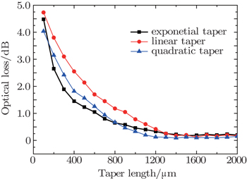
When the length of MMI coupler is fixed at 4050 μm and the output tapered waveguide adopts the same dimensions as the input one, a comparison of the optical loss changing with the variation of tapered waveguide length is shown in Fig. 4. All these tapers show steady loss decrement with the length increasing. When the length of transition waveguide is over 1400 μm, the optical loss of quadratic transition waveguide, which is below 0.1 dB, is lower than that of a linear or exponential taper. Linear taper provides the largest insertion loss even at the length of 1200 μm. These results originate from the fact that power coupling in the quadratic taper is stronger than that in the other two tapers, especially for a short transition waveguide that needs to convert the optical power from higher orders to the fundamental order, mostly. Moreover, the fast and strong power coupling between the fundamental mode and higher orders in the quadratic taper results in a relatively short MMI waveguide. Therefore, a 1400-μm-long quadratic taper is adopted in this design, which compromises the insertion loss with power stability.
Fig. 4. Comparison of the insertion loss induced by different tapers with the variation of length.
3. Simulations
3.1. Thermal diffusion
Thermal characteristics of the attenuator, including thermal diffusion and steady-state response evaluation, can be studied by solving the following heat transfer Fourier’s equation in transient condition with constant thermal conductivity:[22]
where Q(x, y, z, t) is the heat generation rate per unit volume, ρ is the material density, cp is the heat capacity, and k is the thermal conductivity. The initial temperature T is assumed to be 300 K on the cladding and bottom surface, and the boundary conditions can be described as
Equation (4) is the boundary condition between air and P(MMA–GMA) cladding, where h is the natural convection heat transfer coefficient and TA is air temperature. Equation (5) represents the internal boundaries, where k1 and k2 are the thermal conductivities of silicon substrate and waveguide materials. Parameters used in the finite element method calculation according to Eqs. (4) and (5) are listed in Table 1. Here, the silicon substrate and top surface are assumed to be an efficient heat sink and exposed to still air at room temperature.
Table 1.
Table 1.
Table 1.
Material parameters used in thermal calculations.
.
SU-8
P(MMA–GMA)
SiO2
Si
ρ/kg·m−3
1190
1200
2200
2330
cp/J·kg−1·K−1
1200
1420
730
703
k/W·m−1·K−1
0.2
0.2
1.4
163
Table 1.
Material parameters used in thermal calculations.
.
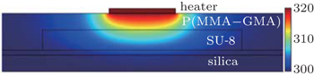
When a certain driving power is applied to the heater, the calculated steady state of heat distribution across the section of VOA waveguide is shown in Fig. 5. While working, the temperature generated by the application of electrical power on the heater exhibits a maximum close to the heater and reduces gradually from it. It is well known that the polymer has a negative expansion coefficient that the refractive index decreases with the rising temperature. Hence, the temperature gradient in P(MMA–GMA) cladding results in a negative gradient of refractive index below the metal stripe. The optical output of the attenuator would be controlled by varying the temperature gradient formed in the device by electrical heating. A relatively low heating power would be required to achieve the desired index change when the polymer has a more negative thermo–optic coefficient.
Fig. 5. Steady-state thermal distribution in the activity waveguide cross-section.
3.2. Switching performance
Thermal analysis allows evaluation of the power consumption by analyzing the power dissipation per unit length that is required to get a certain temperature difference.[23] It is reasonable to demonstrate that this power is proportional to the thermal conductivity
where ΔT is the difference between the initial and final stationary states. Therefore, the relationship between heater power consumption P and heater temperature can be expressed by the following expression:[24]
where Le ≈ L is the length of electrode, We = 8 μm is the electrode width, and h is the thickness of core and cladding layers.[25] Beam propagation method is adopted to investigate characteristics of attenuation with the heating power. As shown in Fig. 6, different α angles are used to investigate their impacts on the reflection. The power consumption of 18.5 mW at 27.5 dB attenuation and 32 mW at 33 dB are estimated for 1.5˚ and 2˚, respectively. When the heater is placed at different α angles with respect to the mode propagation direction, the electrical power induced temperature and refractive index gradients inside polymers also change. This will lead to the difference of reflected light that will be coupled back into higher-order guiding modes. Since these higher-order guiding modes will be filtered out ultimately by the output tapered region and the single-mode output waveguide, the final optical power received from the output single-mode waveguide varies with the heater placement angle. Moreover, the driving power of the heater with different α angles varies at the maximum attenuation, because the mode field distributions change as propagating as shown in Fig. 7.
Fig. 7. Schematic of non-attenuation (a) and maximum attenuations when heaters are placed at α angles of 1˚ (b), 1.5˚ (c), and 2˚ (d) with respect to the mode propagation direction.
Considering the thermal field distribution across the waveguide and its modulating behavior, the heater is placed with an optimized angle α = 1.5˚ on the top cladding, which is a compromise between the power consumption and attenuation range. The fluctuation of power consumption in Fig. 6 is due to the mode interference in the output transition region.
4. Device fabrication and characterization
Firstly, a layer of 3-μm-thick silica was formed on the silicon substrate by thermal oxidation method as the bottom-cladding. A layer of 3-μm-thick SU-8 (Microchem Co., USA) was spin-coated over the bottom-cladding at 3500 rpm and baked for 10 min at 65 ˚C, 20 min at 90 ˚C to evaporate the solvent, respectively. After being UV cured by a mercury (Newport Co., 10 mW/cm2 at 365 nm) lamp for 30 s, it was hard baked at 95 ˚C for 30 min. Then, the SU-8 cross-linked sufficiently, exhibiting excellent chemical and thermal stability. The photoresist BP212 (Kempur Microelectronics Inc., China) was spin-coated on a thermal deposited metal mask and patterned by UV photolithography machine (ABM Co. Inc., USA) to define VOA waveguide patterns. After that, inductively coupled plasma (ICP) etching was carried out in oxygen atmosphere to form the ridge waveguide. Afterwards, P(MMA–GMA) was spin-coated on the SU-8 core layer at 2500 rpm and subsequently baked at 120 ˚C for 2.5 h to remove the solvent. This upper-cladding can improve the efficiency of guided mode index modulation and decrease the roughness of the film surface after ICP processing. Finally, a layer of 600-nm Al film was thermally evaporated and patterned with UV photolithography. Wet etching was adopted to form a heater aligned on the upper-cladding. Before the measurement, the sample device was sliced by a wafer dicing machine DAD-3220 (DISCO Co. Inc, Japan) to reduce fiber-coupling-induced optical loss. The optical microscope image of Fig. 8 shows the top view of the fabricated VOA. Figure 8(a) presents the ridge waveguide structure with vertical profile of the single-mode output waveguide, which is favorable to mode light field confinement and reducing the optical loss. Figure 8(b) shows the scanning electron micrograph image of the cross-sectional state of multimode waveguide section.
Fig. 8. Optical microscope image of the fabricated attenuator. The inset (a) presents the ridge waveguide structure with vertical profile of the single-mode output waveguide; inset (b) shows the cross-sectional state of multimode waveguide section by scanning electron micrograph.
5. Measurement and discussion
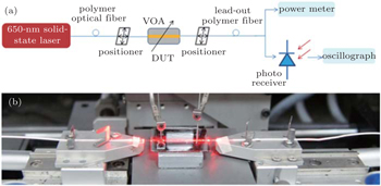
The measurement setup of transmission and switching performances for the fabricated thermal VOA is shown in Fig. 9(a). The end-fire excitation method is adopted to guide the visible light wavelength along the waveguide.[5] A light beam (at λ = 650 nm) from a solid-state laser is directly launched into the input waveguide of the attenuator through a customized small-diameter polymer optical fiber. A similar polymer fiber is used to couple the output signal to an optical power meter to monitor the insertion loss change. The optical output is optimized through aligning the output fiber with a five-axis position controller, as well as the input fiber alignment. The oscillograph connected to a photo receiver is used to observe and record the dynamic performance of the attenuator. The device is fixed on a thermal controller to maintain its temperature at 22 ˚C. The electrical current is introduced to the attenuator through electrode pads contacting with two needle-like probes. Figure 9(b) shows the photograph of the device under test.
Fig. 9. (a) Measurement setup of transmission and switching performances for VOA, (b) photo of VOA under test with fiber alignment system.
5.1. Attenuation
The measured attenuation characteristics at a wavelength of 650 nm are shown in Fig. 10, which approximately agrees with the simulated results in Fig. 6. The insertion loss of a fabricated 1-cm-long attenuator without applying voltage is 6.8 dB. The propagation loss that results from the material imperfection and ICP etching-induced side wall roughness is measured to be about 1.8 dB/cm by cut-back method.[26] The coupling loss is 2.5 dB/facet. The uncertainty of the measurement is proven to be less than 0.5 dB/cm due to the repeatability of chip cleaving. When the electrical current is input through contact pads, the generated temperature grade substantially induces refractive index perturbation in MMI waveguide. As shown in the figure, the electrical power to obtain the maximum attenuation of 26.5 dB is about 21 mW, which is larger than the calculated value due to the dimension difference between the fabricated and designed one. Correspondingly, ΔT can be deduced from Eq. (7) and device parameters used in Sections 2 and 3. The result shows a temperature increment of 10.5 K at the heater power consumption of 21 mW. Since the thermo–optic coefficient of P(MMA–GMA) is about −1.2 × 10⁻⁴ K−1, its refractive index will decrease from 1.510 to 1.5088 when the VOA has the largest attenuation of 26.5 dB. Though SU-8 has a different negative thermo–optic coefficient of −1.8 × 10⁻⁴ K−1, its refractive index will also decrease due to the temperature gradient in polymers. A small change of refractive index of polymers will induce remarkable phase shift of the propagating mode for attenuators based on MZI law. Here, the heater is to form deep contrast of refractive index inside the MMI waveguide. Therefore, a higher power consumption is required. However, this MMI waveguide design is more fit for large scale integration, because it relaxes the requirement for the environmental temperature stability and improves the flexibility for on-chip integration with other optical devices.[16,27]
Fig. 10. Experimental attenuation characteristic versus electrical power of the fabricated attenuator at the wavelength of 650 nm.
5.2. Time stability
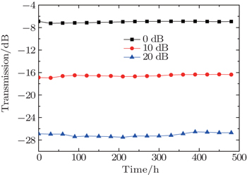
The intrinsic volume relaxation of polymers might affect the optical performance of an interference-based attenuator during its service life. Moreover, the large thermo–optic coefficient of polymer material makes this attenuator possibly to be temperature-dependent. Therefore, the device working stability is tested under different attenuation levels within 480 h, as shown in Fig. 11. When no voltage is applied, the change of loss is less than 0.35 dB. At attenuation level of 10 dB, the loss variation is still less than 0.4 dB, which is mainly owing to the inorganic silica bottom-cladding with high thermal conductivity. However, a loss change of about 0.6 dB is observed at an attenuation of 20 dB. This increased loss change observed at higher attenuation level is partly due to the variation of the thermo–optic coefficient of polymers at an increased temperature. Besides, the resistivity variation of metal heater may be another cause of unstable working. An optical feedback circuit can be adopted to restrain the temperature dependence of this VOA.[8] In fact, this measurement is carried out because these data can be applied to Arrhenius equations to predict the working status of VOA. Due to the chemical property of the polymer, the time variation of insertion loss characteristics of SU-8 and P(MMA–GMA) can be evaluated by popular kinetic mode of Arrhenius equations model and the lifetime of the device can be predicted.[28]
Fig. 11. Measured transmission characteristics of the insertion loss as a function of time.
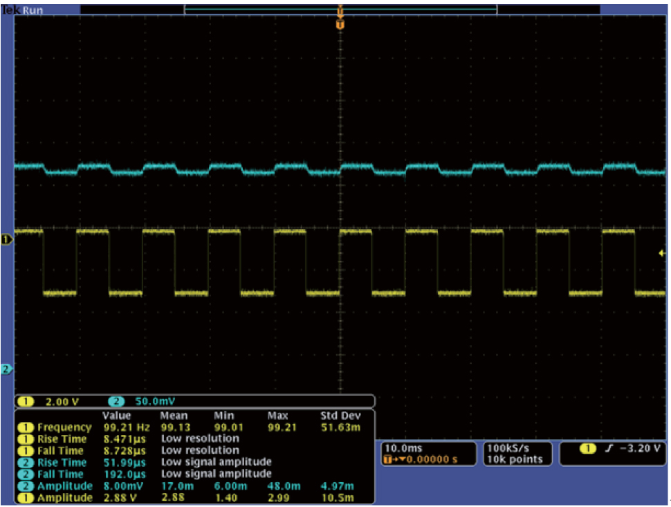
5.3. Time response
As mentioned before, the time response is measured by an oscilloscope DPO4104B (Tektronix Inc., USA) through collecting the output optical power with a polymer fiber, which is connected to an optical power meter. Here, the rise time and fall time are defined as the time that the detected optical power increases from 10% to 90% or decreases from 90% to 10% of its peak value, respectively. When a 100-Hz square waveform drive current is applied to the heater, the measured optical rise time and fall time are 51.99 and 192 μs, respectively, as shown in Fig. 12. The upper trace is the square wave form of the applied voltage source, and the lower trace is the response from the output waveguide. It is known that the rise time and fall time are mainly determined by the time that heat transfers from the top heater to the silicon substrate. Therefore, the fact that the fall time is larger than the rise time can be explained as the construction of temperature grade in polymer cladding being faster than the refractive index restore process. Since the heat transfer process relates to the slab thickness between the heater and substrate, reducing the thicknesses of the core and cladding layers under the condition of single-mode propagation is an effective way to improve the time response performance. In fact, the thicknesses of P(MMA–GMA) or silica can be decreased possibly to construct a shorter distance for heat dissipating toward the substrate because of the index contrast between the core and cladding layers. Besides, the adoption of material with larger thermal conductivity than that of the P(MMA–GMA) as the upper-cladding can reduce the heat dispatch/transfer time further.
Fig. 12. Time response of the polymer/silica waveguide thermal VOA.
Comparing performances of reported attenuators based on TO effect,[14–16] polymeric VOA has the lowest power consumption of less than 10 mW, however, the longest response time. Since the thermal conductivity of silica is six times larger than that of polymers, the generated heat will transmit to the silicon substrate more quickly than using the polymer as the bottom-cladding. Hence, this attenuator costs less time to realize heat diffusion, and the response time is shorter than that of the whole polymeric VOA. However, compared to silica as the bottom-cladding, all polymer waveguide configurations can reduce the power consumption due to the relatively small thermal conductivity. Therefore, a tradeoff between the power consumption and response time needs to be balanced and it is desirable to adopt a complex waveguide configuration to realize a desired device response. Besides, the small device dimensions of less than 1 mm in length and 24 μm in width features compactness, and the resulting low insertion loss of 6.8 dB provides good potential of this VOA for planar lightwave chip applications.
6. Conclusion
In this paper, a 650-nm visible-light attenuator based on polymer/silica hybrid waveguide is designed and experimentally demonstrated. The mode propagation condition and transition waveguide are optimized through EIM and BPM methods. Thermal analysis provides the optimal metal heater angle. The attenuation characteristics are numerically investigated. Experimental characterization of the fabricated device presents an attenuation of 26.5 dB with 21-mW electrical input power at 650 nm. Fast response (rise time and fall time are 51.99 μs and 192 μs, respectively) is observed due to the adoption of silica bottom-cladding with relatively large thermal conductivity. In addition, the measured working stability proves this device can satisfy the reliability requirements for telecom components.
The 650-nm variable optical attenuator based on polymer/silica hybrid waveguide
[Yu Yue-Yang1, Sun Xiao-Qiang1, 2, †, , Ji Lan-Ting1, He Guo-Bing1, Wang Xi-Bin1, 2, Yi Yun-Ji1, 2, Chen Chang-Ming1, 2, Wang Fei1, 2, Zhang Da-Ming1, 2]


 , Ji Lan-Ting1, He Guo-Bing1, Wang Xi-Bin1, 2, Yi Yun-Ji1, 2, Chen Chang-Ming1, 2, Wang Fei1, 2, Zhang Da-Ming1, 2]