Yu Jun-Ting, Chen Shu-Ming, Chen Jian-Jun, Huang Peng-Cheng, Song Rui-Qiang. Effect of supply voltage and body-biasing on single-event transient pulse quenching in bulk fin field-effect-transistor process. Chinese Physics B, 2016, 25(4): 049401
Permissions
Effect of supply voltage and body-biasing on single-event transient pulse quenching in bulk fin field-effect-transistor process
College of Computer, National University of Defense Technology, Changsha 410073, China
National Laboratory for Parallel and Distributed Processing, National University of Defense Technology, Changsha 410073, China
† Corresponding author. E-mail: smchen_cs@163.com
Project supported by the National Natural Science Foundation of China (Grant Nos. 61376109, 61434007, and 61176030).
Abstract
Abstract
Charge sharing is becoming an important topic as the feature size scales down in fin field-effect-transistor (FinFET) technology. However, the studies of charge sharing induced single-event transient (SET) pulse quenching with bulk FinFET are reported seldomly. Using three-dimensional technology computer aided design (3DTCAD) mixed-mode simulations, the effects of supply voltage and body-biasing on SET pulse quenching are investigated for the first time in bulk FinFET process. Research results indicate that due to an enhanced charge sharing effect, the propagating SET pulse width decreases with reducing supply voltage. Moreover, compared with reverse body-biasing (RBB), the circuit with forward body-biasing (FBB) is vulnerable to charge sharing and can effectively mitigate the propagating SET pulse width up to 53% at least. This can provide guidance for radiation-hardened bulk FinFET technology especially in low power and high performance applications.
With technology scaling beyond 22-nm node, traditional planar transistors are vulnerable to undesirable short channel effects (SCEs), which present the most important constraints to complementary metal–oxide–semiconductor (CMOS) scaling rules. Owing to the superior electrostatic scalability and better gate controllability over the channel (fin), Fin field-effect-transistors (finFETs) are widely recognized as a most promising candidate for traditional bulk CMOS transistors.[1,2] As a consequence, FinFET technologies are currently becoming the mainstream process in the leading semiconductor manufacturers.[3]
The pulse quenching has been reported in CMOS logical circuits and is widely identified as the result of multi-node charge collection between the electrically related transistors.[4–6] This would reduce the propagated single-event transient (SET) pulse width, which is beneficial to reducing the soft errors.[7,8] Much work has been done to investigate the pulse quenching in planar CMOS logic circuits.[9–12] As the feature size of transistor and space between devices scale down, the charge sharing effect (also called the multi-node charge collection) is becoming an important topic in FinFET technology.[13,14] However, to the best of our knowledge, little work has been done on the SET pulse quenching in those novel FinFET devices. Besides, with the reducing supply voltage as technology scales down, body-biasing has become an efficient control technique for optimizing the performance and power of devices.[15,16] The charge collection and well potential will also be affected by body-biasing when a single-event occurs in the circuit.[17] Thus, it is important to analyze the effects of body-biasing on charge collection and the resulting SET pulse quenching in the FinFET process.
In the present work, 3D TCAD mixed-mode simulations are performed to investigate the influences of supply voltage and body-biasing on the pulse quenching effect in a two-stage inverter chain in bulk FinFET process. Simulation results show that the SET pulse propagated to the passive p-FinFET decreases with supply voltage decreasing. Moreover, compared with the reverse body-biasing (RBB) circuit, the forward body-biasing (FBB) circuit is vulnerable to charge sharing and exhibits a mitigation of the propagating SET pulse about 53% at least. The rest of this paper is organized as follows. In Section 2 the TCAD simulation setup is presented. In Section 3 the simulation results are provided and the influences of supply voltage and body-biasing on SET pulse quenching are discussed. Finally, the conclusions are drawn from the present study in Section 4.
2. Simulation setup
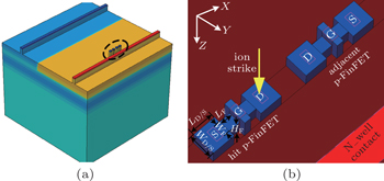
Synopsys Sentaurus TCAD H-2013.03-SP1 is employed to investigate the effects of supply voltage and body-biasing on the pulse quenching in a two-stage inverter chain under bulk FinFET process. Figure 1 shows the 3D TCAD model of two bulk p-FinFETs in the dual-well process. For the simulated p-FinFET device, the gate oxide is 1.2-nm thick and the gate work function used is a default value (4.9 eV for p-Si). The doping concentrations of the source region and the drain region are both 1020 cm−3. The peak doping levels in the fin (channel) and N-well are 1018 cm−3 and 1017 cm−3, respectively. Table 1 shows the geometrical structure parameters of the p-FinFET. The FinFET device is calibrated with reference to the I–V characteristics of a planar device under the 28-nm process.
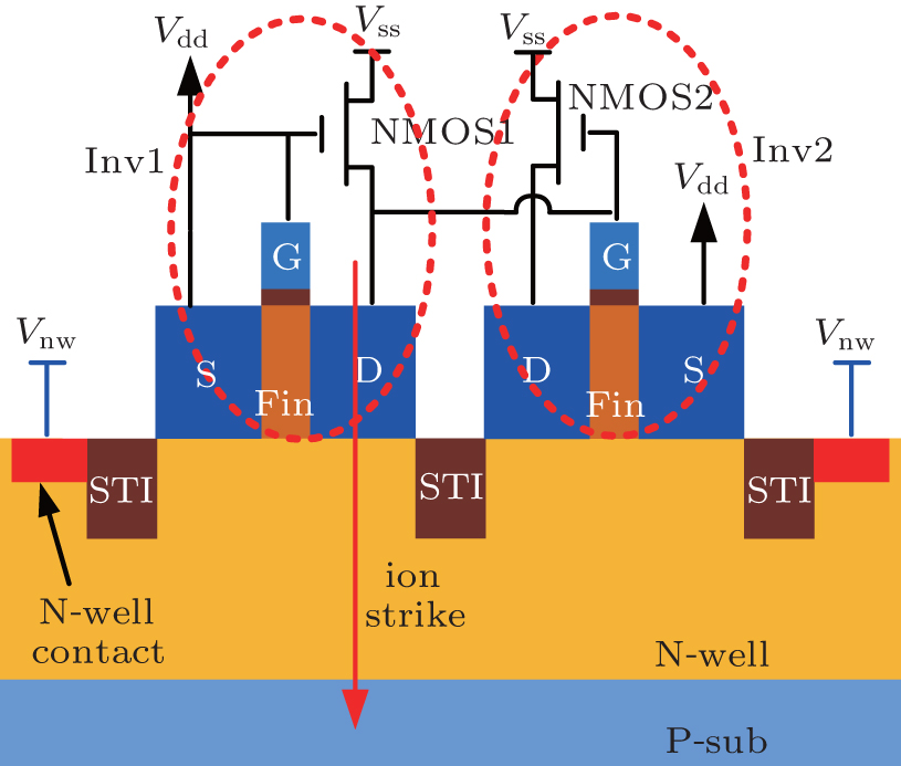
Fig. 2. Schematic configuration of the mixed-mode simulation setup for a two-stage inverter chain. The TCAD p-FinFETs are cut in the middle of the gate along the source/drain direction (X–Z plane).
As illustrated in Fig. 2, the mixed-mode simulation setup for a two-stage inverter chain is comprised of two TCAD p-FinFET devices and two NMOS SPICE models. The p-FinFET in the first stage (Inv1 from Fig. 2) represents the hit device while the p-FinFET in the second stage (Inv2 from Fig. 2) represents the adjacent device. The gates of Inv1 and Inv2 are separately biased at supply voltage Vdd and the output of the Inv1, respectively. The source of the p-FinFET device is biased at Vdd. The N-well contact is related to a voltage defined as Vnw. In our simulation, the voltage difference (Vsb) between Vdd and Vnw is referred to as the body-biasing. Based on the voltage difference, forward body-biasing (FBB) involves applying a positive value, while the reverse body-biasing (RBB) refers to a negative one.
In the following sections, the p-FinFET struck by heavy-ion is defined as the active device, while the adjacent p-FinFET is termed the passive device. The space between the active and passive FinFETs is 120 nm, and simulations are conducted for normal strike on the drain center of the active device with an ion linear energy transfer (LET) value of 20 MeV·cm2/mg. The following physical models are used in the simulations: 1) Fermi–Dirac carrier statistics; 2) band-gap narrowing effect; 3) doping-dependent Shockley–Read–Hall (SRH) and Auger recombination; 4) effects of temperature, doping, electric field, and carrier–carrier scattering on mobility; 5) a hydrodynamic model is used for the carrier transportation equations; and 6) incident heavy ions are modeled by using a Gaussian radial profile with a characteristic 1/e radius of 50 nm and a Gaussian temporal profile with a characteristic decay time of 0.25 ps.
3. Simulation results and discussion
3.1. Influence of supply voltage on SET pulse width
In this simulation, the N-well contact is connected to the supply voltage Vdd (also called zero body-biasing (ZBB)), and the circuit with different supply voltages varying from 0.7 V to 1.1 V is simulated to investigate the voltage dependence of SET pulse width.
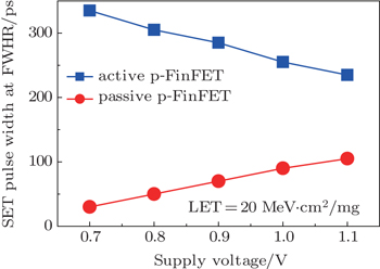
Figure 3 shows the simulated results. It can be seen that the SET voltage at the full width of half rail (FWHR, which is also called pulse width) captured at the active p-FinFET decreases with supply voltage increasing, while the SET pulse propagating to the passive device exhibits an opposite voltage dependence trend. The reason behind this can be analyzed as follows.
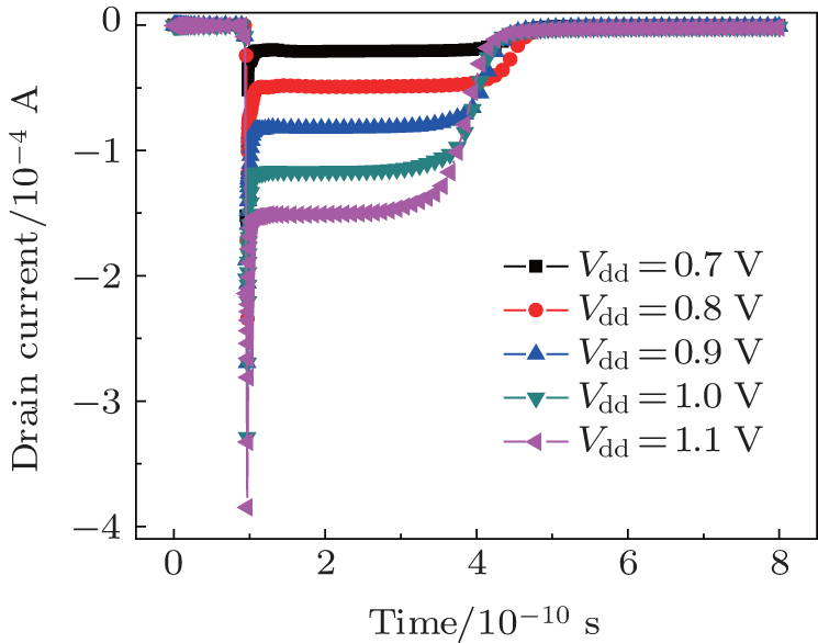
As shown in Fig. 4, the drain current transient in the active p-FinFET increases as the supply voltage varies from 0.7 V to 1.1 V, which indicates a prompt discharged current through the complementary NMOS1 transistor. Moreover, the increased supply voltage (Vdd) is connected to the N-well contact and this can quickly collect the single-event generated charge (electron) and further lead to a faster well potential recovery. As a result, the SET pulse width decreases with supply voltage increasing. This is consistent with the result in a planar CMOS circuit.[10,18,19]
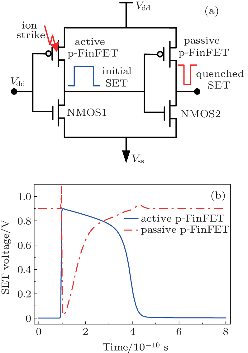
Fig. 5. (a) A schematical configuration of two-stage inverter chain showing the initial and quenched SET pulse signal after an ion strike; (b) simulated SET pulse quenching in the two-stage inverter chain. The ion LET is 20 MeV·cm2/mg.
However, the SET pulse propagating to the passive p-FinFET increases with supply voltage increasing from 0.7 V to 1.1 V, which exhibits an opposite voltage dependence trend compared with the case in an active device. This can be explained by the single event charge sharing and the resulting pulse quenching effects between the proximal nodes which are electrically related to each other. As described in Ref. [4], the pulse quenching is determined by the competing mechanism between propagating SET electrical signal and the charge sharing induced SET pulse of the passive device. Owing to the reduced nodal spacing and high packing density in FinFET technology, a charge sharing effect occurs easily between the FinFET transistors. Figure 5 shows a schematical configuration of the two-stage inverter chain and the simulated result of SET pulse quenching in this work. It can be seen that the SET pulse propagating to the passive device is truncated much more than that generating in the active device after an ion strike.
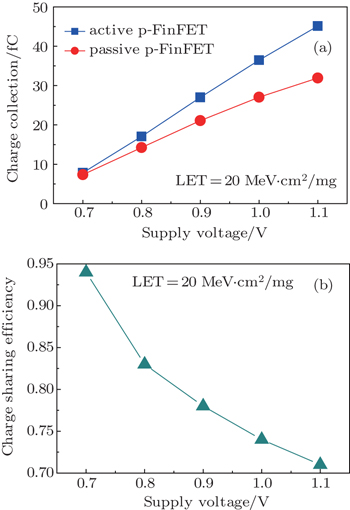
A great deal of work has highlighted the relationship between the SET pulse and the amount of charge collection in an inverter chain, which shows that when the voltage applied to the complementary transistor is fixed, the SET pulse width is proportional to the charge collection. To ensure that the charge collected in a passive device is caused by the charge sharing effect, the same circuit configuration and hit location as shown in Fig. 2 are used, but in the opposite logical state (that is, the active p-FinFET ON while the passive p-FinFET OFF). Here, a parameter termed charge sharing efficiency (CSE) is defined as the ratio of the charge collected by the passive device to that collected by the active device, which is used firstly to illuminate the effects of supply voltage and body-biasing on the SET pulse propagating to the passive device.
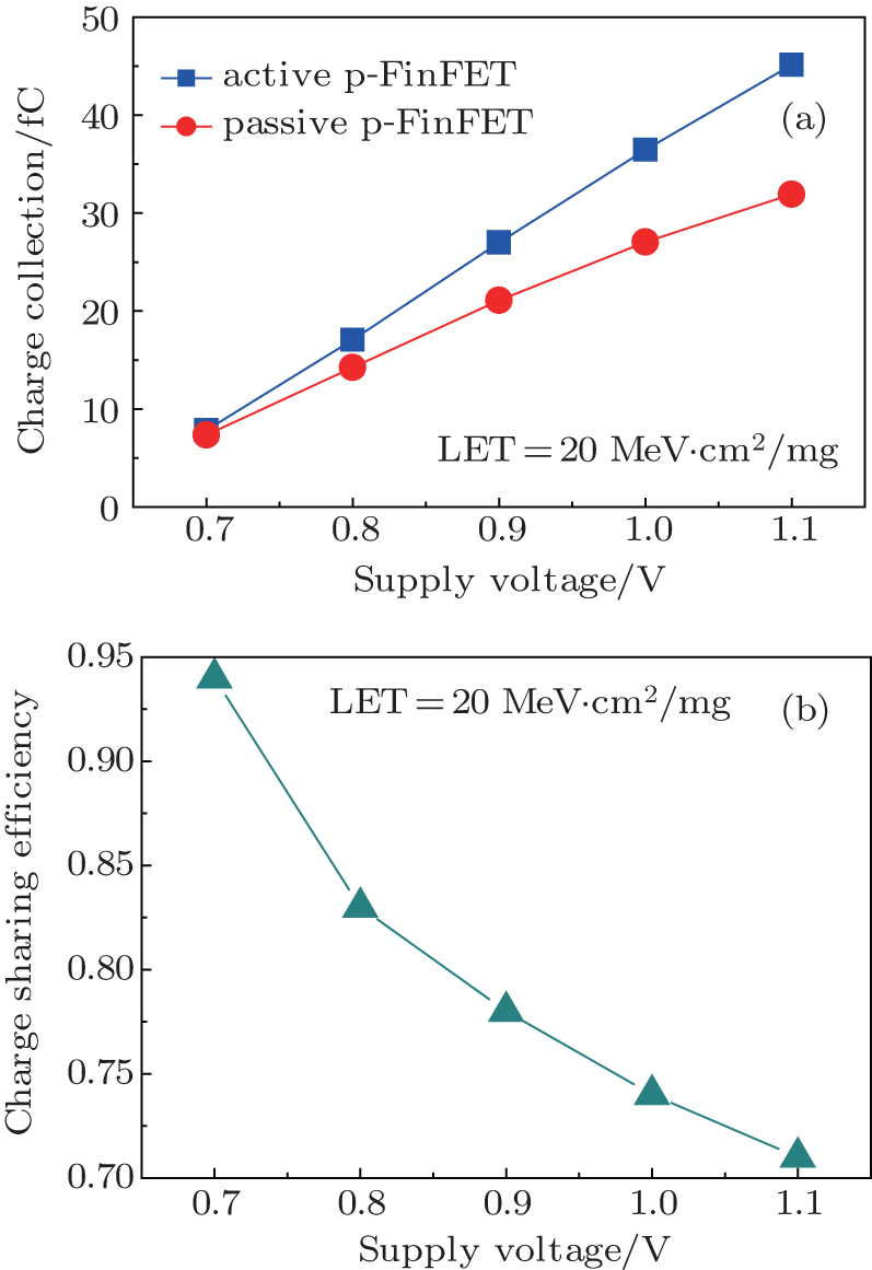
Figures 6(a) and 6(b) clearly show the variations of charge quantities collected in active and passive p-FinFETs and the corresponding CSE factor with supply voltage respectively. It can be observed that the charge quantities collected by the active and passive devices increase with supply voltage. However, the CSE decreases as supply voltage increases from 0.7 V to 1.1 V. As mentioned previously, owing to a prompt discharged current through the complementary n-MOSFET at higher supply voltage, the SET pulse in the active FinFET decreases as Vdd varies from 0.7 V to 1.1 V. Moreover, the reduced CSE results in a quick decrease of the SET pulse induced by charge sharing in the passive p-FinFET. As is well known, the quenched pulse propagating to the passive p-FinFET is determined by subtracting the charge sharing induced SET pulse from the pulse generated in the active device. Thus, the SET pulse propagating to the passive device increases with the supply voltage varying from 0.7 V to 1.1 V.
Fig. 6. (a) Plots of (a) charge quantities collected in active and passive p-FinFETs and (b) the corresponding charge sharing efficiency versus supply voltage, with the ion LET being 20 MeV·cm2/mg.
3.2. Effect of body-biasing on SET pulse quenching
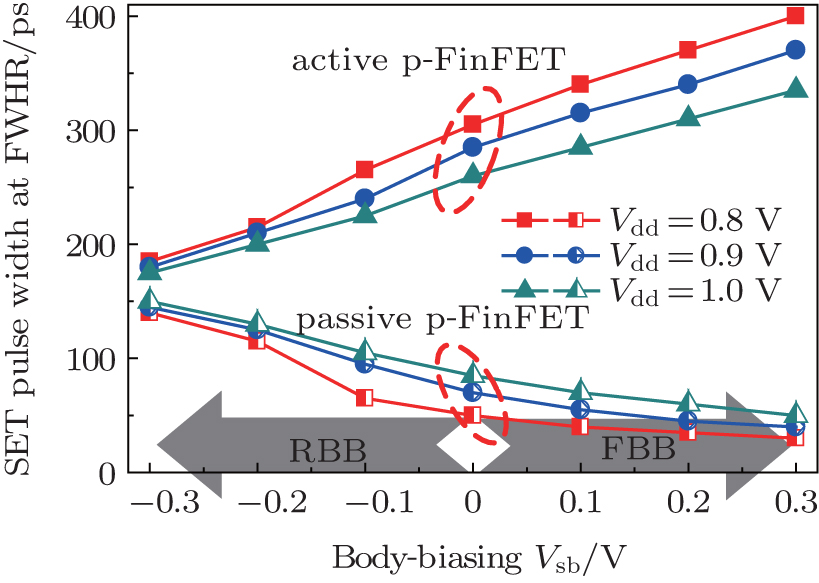
In this simulation, the N-well contact is biased at a voltage separated from Vdd. The circuits with different body-biasing modes (FBB, RBB, and ZBB) are simulated to investigate the effect of body-biasing on the SET pulse quenching in the bulk FinFET process. The bias voltage varies from −0.3 V to 0.3 V. That is, the negative value refers to RBB, while the positive value corresponds to FBB.
The simulated results are shown in Fig. 7. It can be seen that the SET pulse propagating to the passive p-FinFET decreases as body-biasing varies from RBB to FBB. This can be explained in terms of the enhanced charge sharing effect between the electrically coupled nodes under FBB condition.
Fig. 7. Variations of SET pulse width at FWHR captured in active and passive devices with body-biasing for three supply voltages (0.8 V, 0.9 V, and 1.0 V). All simulations are conducted with the same ion LET at 20 MeV·cm2/mg.
In our previous work, we illustrated that the bipolar amplification induced by the N-well can exert important effects on the charge collection and SET pulse width in bulk p-FinFETs.[20,21] The body-biasing can affect the potential barrier between the source and N-well, which is a key factor for the parasitic bipolar junction transistor (BJT_Well) to be turned on. The injection hole current from source to the N-well is calculated as[22]
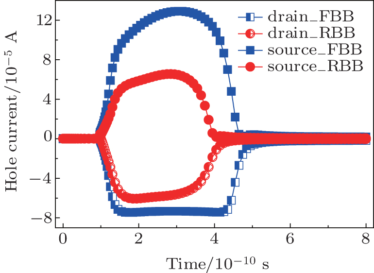
where Vb−e is determined by the voltage applied to the parasitic PN junction (here corresponding to the voltage difference Vsb between the source and N-well). A positive voltage value for the FBB gives a larger hole current than a negative value for RBB, which is further verified by the hole current density profiles in Fig. 8. It indicates that the holes current density either produced from the source or collected by the drain in FBB is much larger than that in RBB. Figure 9 shows that the hole current of drain and source both terminate in the passive p-FinFET with different body-biasing modes for the whole strike time. Consequently, the body-biasing has a significant influence on charge collection and SET pulse.
Fig. 9. Hole currents of drain and source terminating in the passive p-FinFET for different body-biasing voltages at 0.2 V (FBB = 0.2 V, RBB = −0.2 V). The ion LET is 20 MeV·cm2/mg.
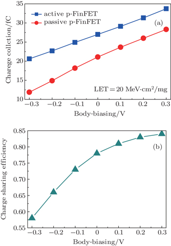
Figures 10(a) and 10(b) show the variations of charge quantities collected in active and passive devices and the corresponding CSE factors with body-biasing voltage respectively. As explained in the last section, the propagating SET pulse is mainly determined by the charge sharing effect. A larger CSE can result in a stronger pulse quenching effect and a reduced propagating SET pulse width. It can be seen that the CSE factor increases as the body-biasing varies from RBB to FBB. As a consequence, the charge sharing induced SET pulse will be larger in the FBB mode, thereby leading to a resulting smaller pulse width in the passive p-FinFET than in RBB.
Fig. 10. (a) Charge quantities collected in active and passive devices and (b) the corresponding charge sharing efficiency versus body-biasing, with the ion LET being 20 MeV·cm2/mg.
As shown in Fig. 11, the body-biasing strategy can be used to mitigate the propagating SET pulse width effectively, especially for the lower LET values. This is more important in the advanced FinFET technology because the critical ion LET required for producing the SET and eventually an SEU is rapidly decreasing with the device scaling down. As discussed earlier and illustrated in Fig. 11, an enhanced charge sharing between the electrically coupled nodes with FBB can result in more than 53% reduction of SET pulse width compared with the one with RBB. This can provide guidance for radiation-hardened bulk FinFET technology especially in low power and high performance applications.
Fig. 11. Comparison among the plots of SET pulse width propagating to the passive p-FinFET for different body-biasing modes versus ion LETs.
4. Conclusions
According to the 3D TCAD mixed-mode simulation, we investigate the effects of supply voltage and body-biasing on the SET pulse quenching in bulk FinFET process. The proposed CSE factor is used to determine the characteristics of SET pulse width between the active and passive p-FinFETs. According to the simulation results, the SET pulse propagating to the passive device decreases when reducing the supply voltage. The results also indicate that owing to an enhanced bipolar amplification effect, the circuit with FBB is more vulnerable to charge sharing than that with RBB. The propagating pulse in FBB mode is truncated up to 53% compared with that in RBB mode. This is very important in the advanced nano-scale FinFET circuit for the single-event effect, and can provide guidance for radiation-hardened bulk FinFET technology, especially in low power and high performance applications.
Reference
1
ColingeJ P2008FinFETs and Other Multi-Gate TransistorsNew YorkSpringer525652–6(in Chinese)10.1007/978-0-387-71752-4
2
FossumJ GTrivedlV P2013Fundamentals of Ultra-Thin-Body MOSFETs and FinFETsNew YorkCambridge University Press333533–510.1007/978-0-387-71752-4


 , Chen Jian-Jun1, Huang Peng-Cheng1, Song Rui-Qiang1]