Comparison of blue–green response between transmission-mode GaAsP- and GaAs-based photocathodes grown by molecular beam epitaxy
Jiao Gang-Cheng1, 2, †, , Liu Zheng-Tang1, Guo Hui2, Zhang Yi-Jun3
State Key Laboratory of Solidification Processing, School of Materials Science and Engineering, Northwestern Polytechnical University, Xi’an 710072, China
Science and Technology on Low-Light-Level Night Vision Laboratory, Xi’an 710065, China
School of Electronic and Optical Engineering, Nanjing University of Science and Technology, Nanjing 210094, China


† Corresponding author. E-mail: jiaogc613@163.com

Project supported by the National Natural Science Foundation of China (Grant No. 61301023) and the Science and Technology on Low-Light-Level Night Vision Laboratory Foundation, China (Grant No. BJ2014001).

Abstract
Abstract

In order to develop the photodetector for effective blue–green response, the 18-mm-diameter vacuum image tube combined with the transmission-mode Al0.7Ga0.3As0.9P0.1/GaAs0.9P0.1 photocathode grown by molecular beam epitaxy is tentatively fabricated. A comparison of photoelectric property, spectral characteristic and performance parameter between the transmission-mode GaAsP-based and blue-extended GaAs-based photocathodes shows that the GaAsP-based photocathode possesses better absorption and higher quantum efficiency in the blue–green waveband, combined with a larger surface electron escape probability. Especially, the quantum efficiency at 532 nm for the GaAsP-based photocathode achieves as high as 59%, nearly twice that for the blue-extended GaAs-based one, which would be more conducive to the underwater range-gated imaging based on laser illumination. Moreover, the simulation results show that the favorable blue–green response can be achieved by optimizing the emission-layer thickness in a range of 0.4 μm–0.6 μm.

1. Introduction

In the last two decades, negative electron affinity (NEA) GaAsP-based photocathodes are of great technological interest and have found widespread application in various fields such as weak light imaging, high energy physics, astronomical observation and underwater photodetection.[14] As is well known, GaAsP-based photocathodes are divided into two basic types, i.e., reflection-mode (r-mode) cathodes for which the light is incident on the electron emission surface and transmission-mode (t-mode) cathodes for which the light is incident on the back surface.

For the r-mode operation, the GaAsP-based photocathode is a promising candidate as an electron source in the high voltage DC photogun due to its low thermal emittance and fast temporal response time.[5] Recently, by means of strained GaAs/GaAsP superlattice structures, the electron-spin polarization reached as high as 92% with a quantum efficiency exceeding 1%.[6,7] For t-mode operation, because of the high quantum efficiency in the visible spectrum, GaAsP photocathodes serve as core components in various photodetectors. For instance, a new type of hybrid photodiode (HPD) consisting of an 18-mm-diameter GaAsP photocathode and an avalanche diode serving as an anode was developed for the major atmospheric gamma-ray imaging Cherenkov (MAGIC) telescope camera.[8,9] Besides, GaAsP photocathode-based image intensifiers with high blue–green light response can provide effective means for laser illuminating range-gated imaging underwater and ultra-fast single-photon counting.[1012]

Despite many prominent advantages and broad applications, there has been no significant progress over the last few decades in developing high-performance t-mode GaAsP-based photocathodes due to the complexity of the preparation process. Currently, the commercially available photodetectors with using t-mode GaAsP photocathodes, such as the image intensifier, photomultiplier and HPD have only come from two corporations, i.e., Hamamatsu and Intevac.[3] Indeed, the quality of epitaxial GaAsP-based heterojunction materials is extremely crucial to the device performance. As is well known, t-mode GaAsP-based cathode materials from Hamamatsu and Intevac are grown by metal-organic chemical vapor deposition (MOCVD) and vapor phase epitaxy (VPE).[1,13] In this paper, a type of t-mode GaAsP cathode material is tentatively fabricated by molecular beam epitaxy (MBE), and the packed 18-mm-diameter image intensifier including the activated GaAsP photocathode module is fabricated. In order to verify the actual effect of blue–green response enhancement, a blue-extended GaAs photocathode-based image intensifier as a comparison object is also fabricated. Meanwhile, the differences in photoelectric property, spectral characteristic and performance parameter between the two types of photocathodes are analyzed.

2. Experiment
2.1. Structure and growth

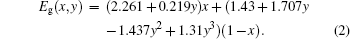
Like the AlGaAs/GaAs double heterostructures described by Antypas and Edgecumbe,[14] the universal inverted structure is applied to the t-mode GaAsP-based photocathodes. However, differing from the lattice-matched AlGaAs/GaAs heterostructure, both heterostructures like GaAsP/GaAs and AlGaAsP/GaAs are lattice mismatched systems. The misfit dislocation and stacking fault arising from the lattice mismatch between substrate and epitaxial layer would dramatically deteriorate the photoemission capability. As for GaAs1−xPx ternary alloy, the dependence of the band gap of GaAs1−xPx alloy on the P composition x is given by[15]

According to Eq. (1), the P composition x should be larger than 0.5 if the cut-off response wavelength is less than 580 nm, which corresponds to the blue–green waveband. Whereas the direct-indirect transition for GaAs1−xPx alloy occurs in approximately 2.0 eV band gap (x = 0.5), and the previous experiment has proved that the quantum efficiency from the NEA GaAsP photocathode drops dramatically as it goes from direct-gap to indirect-gap alloy.[1,16] Consequently, a direct-gap GaAsP alloy with a low P composition of 0.1 is chosen to serve as the emission-layer to ensure the high crystalline quality for epitaxial growth. Besides, an Al0.7Ga0.3As0.9P0.1 quaternary alloy with a band gap of 2.37 eV is chosen to serve as the shortwave window-layer of the t-mode photocathode, and the dependence of the band gap of AlyGa1−yAs1−xPx quaternary alloy on the P composition x and Al composition y can be expressed as follows:[17]

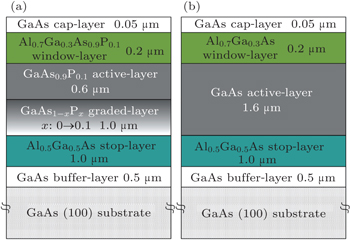
In order to verify the enhancement of the blue–green response for the GaAsP-based photocathode, another type of blue-extended t-mode photocathode consisting of the AlGaAs/GaAs heterostructure was prepared as well. The inverted structures for the two t-mode photocathode samples are shown in Fig. 1, where the different feature for the GaAsP sample is that a GaAsP graded-layer with a variable P composition of 0 ∼ 0.1 is sandwiched between the GaAsP emission-layer and the AlGaAs stop-layer. In the growing of the lattice mismatched AlGaAs/GaAsP heteroepitaxial layer, the graded buffer layers introduced can smooth the transition between them and improve the crystalline quality. The two t-mode cathode samples were both grown on the same 2-inch (1 inch = 2.54 cm) diameter semi-insulation GaAs (100) substrate by using a solid source Riber C21T system equipped with a valved arsenic and phosphorus cracker cell. In the growth process, the epitaxial layers consisting of a stop-layer, an emission-layer, a window-layer, and a cap-layer, were grown according to priority, where the stop-layer and the cap-layer served as an etch-resistant stopping layer and an inside-oxidation-preventing layer, respectively. For the AlGaAs/GaAs cathode material, the growth temperature was kept to be 580 °C for the GaAs layer and 650 °C for the AlGaAs layer. While for the AlGaAsP/GaAsP cathode material, the substrate temperature was always kept at a low temperature of 480 °C for GaAsP and AlGaAsP layers. A 0.5-μm-thick p-GaAs buffer layer was grown to trap impurities that may diffuse from the substrate. To obtain the lattice match structure, a 1-μm-thick undoped GaAs1−xPx graded-layer was grown on the AlGaAs stop-layer. The P composition of the GaAs1−xPx graded-layer was adjusted by P2 flux from zero to the desired flux value. The Ga flux and As flux were kept to be a constant value during the growth. All the samples were cooled down quickly after stopping growth. The beryllium element was incorporated as the p-type dopant for MBE growth and the doping concentration was around 5× 1018 cm−3. During the entire growth procedure, the growth rates for all epilayers were about 1 μm/h, and the crystalline quality of the epilayers was monitored during growth via reflection high-energy electron diffraction in situ.

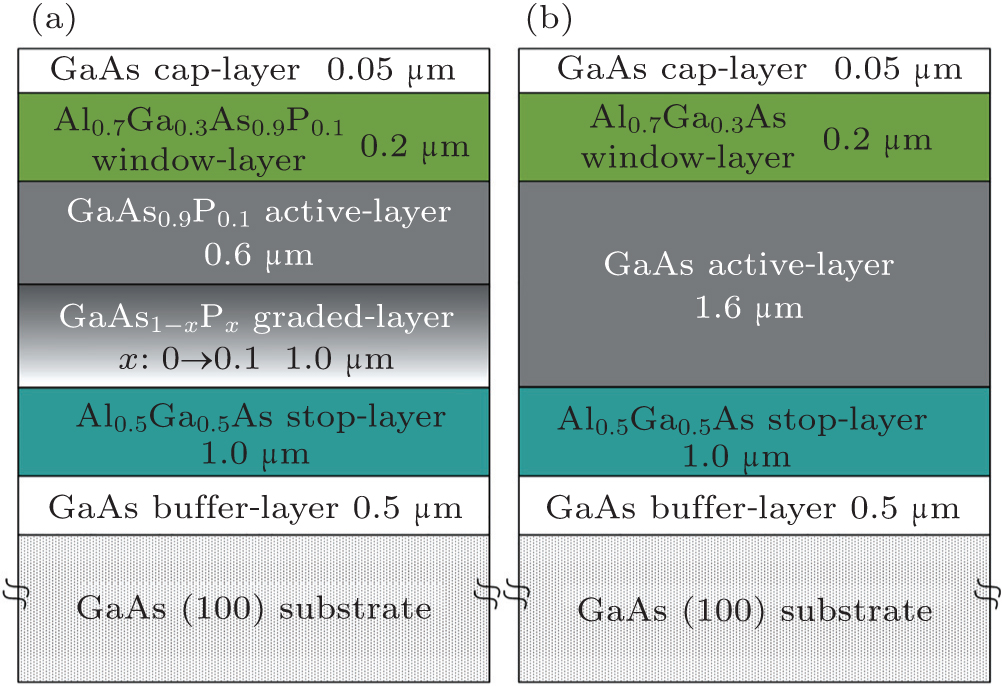
Fig. 1. Structural diagrams of t-mode (a) GaAsP and (b) GaAs cathode samples.
2.2. Preparation and measurement

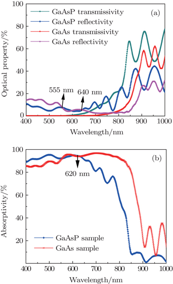
After the growth, the surface photovoltage spectroscopy (SPS) data for the cleaned epitaxial materials were measured to predict the cathode emission performance, since there are many similarities between SPS and spectral response (SR), which are both related to the inherent material performance factors.[18] Following that, as the proposed process of fabricating t-mode GaAs photocathodes by Antypas and Edgecumbe,[14] the cap-layer was first removed with a properly selective etch to expose the window-layer to coat the Si3N4 antireflection film on it. Then the glass was thermocompression bonded to the full wafer structure to support the fragile epilayers. After that, the substrate, stop-layer and graded-layer were selectively etched away to expose the emission-layer to perform the activation. Finally, the AlGaAsP/GaAsP and AlGaAs/GaAs samples were made into the 18-mm-diameter cathode module with a glass/Si3N4/window-layer/emisison-layer structure. Based on the double optical path method, the spectrophotometer typed UV-3600 was adopted to measure the reflectivity and transmissivity curves of the module samples in a range of 400 nm–1000 nm. When measured, photons entered into the modules in the near normal incidence on the glass layer.

Following chemical etching and heat cleaning, the NEA activation for the cathode modules was performed in an ultrahigh vacuum chamber with a base pressure of ≤ 10−9 Pa by using the co-deposition activation technique,[19] in which the cesium source was kept constant and the oxygen source was introduced periodically. For both the samples, the Cs/O flux ratio was adjusted to be the same value. After the usual “high-low temperature” two-step activation, the cathode module was transferred from the activation chamber to the sealed vacuum chamber and indium sealed into a vacuum image tube, in which the activated cathode module was equipped in association with the microchannel plate and fluorescence screen. Finally, the spectral response of the sealed image tube after being transferred into ambient air was measured by the spectral response measurement system.[20]

3. Results and discussion
3.1. Photoelectric property

The experimental curves of optical properties are given in Fig. 2 for the GaAsP- and GaAs-based cathode module samples, and the absorptivity curves are easily gained according to the principle of energy conservation. As shown in Fig. 2(a), in a range of 400 nm–555 nm, the reflectivity of the GaAsP sample is evidently lower than that of the GaAs sample, while the transmissivities for both samples are equal to zero. In a region of 600 nm–950 nm, the reflectivity and transmissivity of the GaAsP sample become larger than those of the GaAs sample. On account of the multi-beam interference principle in the four-layer module, a group of alternative extreme points emerge simultaneously in the reflectivity and transmissivity curves. The maximum point in the reflectivity curve corresponds to the minimum one in the transmissivity curve when taking the energy conservation into consideration. Compared with the GaAs sample, the GaAsP sample produces a big effect on the oscillation frequency of reflectivity. Especially in a waveband of 640 nm–1000 nm, the number of peak-valley cycles in the reflectivity curve for the GaAsP sample greatly exceeds that for the GaAs sample. As shown in Fig. 2(b), in the near-infrared (NIR) band, the GaAsP photocathode gradually becomes optically transparent as the absorptivity decreases to nearly zero. In addition, it can be clearly seen from Fig. 2(b) that the absorptivity of the GaAsP sample is larger than that of the GaAs sample over the blue–green waveband. In the region larger than 620 nm, the absorptivity of the GaAsP sample decreases severely and exhibits a smaller longwave cut-off in contrast with the GaAs sample. Accordingly, it is concluded that the t-mode GaAsP and GaAs samples each manifest better absorptions of blue–green light and red-NIR light, respectively.

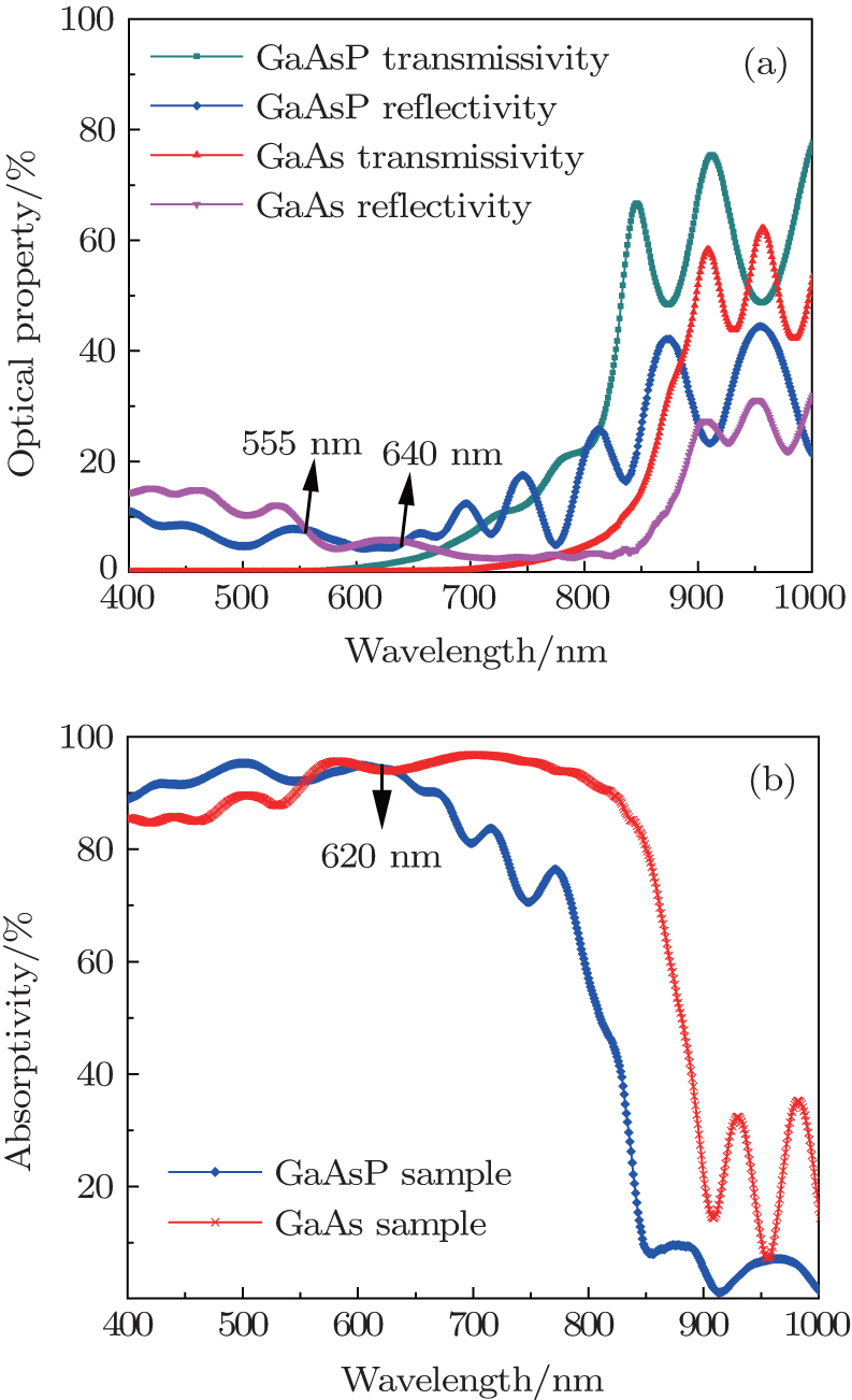
Fig. 2. Experimental optical property curves of t-mode GaAsP and GaAs cathode samples.

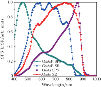
Using the monochromator combined with a tungsten halogen lamp, the measured normalized SPS and SR curves for the two samples are shown in Fig. 3. According to the results shown in Fig. 3, we can find that there are similarities between SPS curves and SR curves, wherein SPS and SR curves possess the same variation trends. The peak wavelengths of SPS and SR curves are in the region of the blue–green spectrum for the GaAsP sample, and in the region of the NIR spectrum for the GaAs sample. It is noted that there exists a difference in peak wavelength between SPS and SR curves. For the GaAsP sample, the peak wavelength of SR is longer than that of SPS while the case for the GaAs sample is the opposite. Since SPS represents the change of potential distribution at the interface of the material due to illumination, the SPS signal of the t-mode multilayer sample is considered to be induced in the surface space charge region (SCR) and at several buried interfaces via light absorption. The reason for the difference is that the SPS signal of the t-mode cathode sample is an algebraic sum of the signals accumulated in the surface SCR and the five interface SCRs,[18] while the SR signal only comes from the photoelectrons in the bulk emission-layer via light absorption. By comparing the SPS curve with the SR curve, it is inferred that for the t-mode GaAsP photocathode, the high SPS in the region of the blue–green spectrum can predict the better SR in the same spectrum region to some extent.

Fig. 3. Normalized SPS and SR curves of t-mode GaAsP and GaAs cathode samples.
3.2. Quantum efficiency

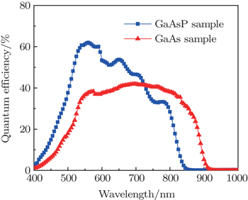
The experimental quantum yield curves for the t-mode GaAsP- and GaAs-based cathode samples sealed in the vacuum image tubes are shown in Fig. 4, which are obtained through converting the spectral response curves.[20] The measured results show that the t-mode GaAsP photocathode can obtain higher quantum efficiency in a range of 400 nm–720 nm, and the longwave cut-off wavelength is at 850 nm. For the t-mode GaAs photocathode, the quantum efficiency in the longwave region is more than 720 nm, and the longwave cut-off wavelength can extend to 920 nm. Although the thin window and high Al composition are applied to the t-mode GaAs photocathode to enhance the shortwave response,[21] the blue–green response of interest is still higher for the t-mode GaAsP photocathode. The GaAsP sample possesses a quantum efficiency peak of 62% at 560 nm while the GaAs sample possesses a quantum efficiency peak of 42% at 690 nm. Besides, the quantum efficiencies at 532 nm reach 59% and 30% for GaAsP and GaAs samples, respectively.

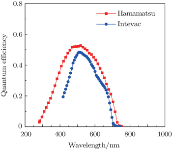
The quantum efficiency curves of foreign t-mode GaAsP photocathodes from Hamamatsu and Intevac are shown in Fig. 5,[1,22] and the spectral characteristics of the t-mode GaAsP photocathodes are shown in Table 1. From Fig. 5 and Table 1, we can see that the comparison of the quantum efficiency curve between the t-mode GaAsP photocathodes from Hamamatsu and Intevac, and the t-mode GaAsP photocathode reported in the present work exhibits that the former has a quantum efficiency peak 62% higher than the latter one at 560 nm. Owing to the high P composition exceeding 0.35, the peak wavelength positions of the t-mode GaAsP photocathodes from Hamamatsu and Intevac are less than the GaAsP photocathode reported in this work. Meanwhile, the t-mode GaAsP photocathode reported in this work, with the lower P composition, has a larger longwave cut-off wavelength. Whereas, the quantum efficiency at 532 nm of our t-mode GaAsP photocathode is higher than that of the ones from Hamamatsu and Intevac, and can reach as high as 59%, which is beneficial to the underwater range-gated imaging based on 532 nm-laser illumination.

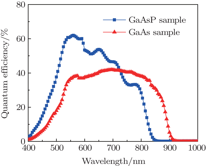
Fig. 4. Experimental quantum efficiency curves of t-mode GaAsP and GaAs cathode samples.
Fig. 5. Quantum efficiency curves of t-mode GaAsP photocathodes from Hamamatsu and Intevac.
Table 1.

Spectral characteristics of this work and t-mode GaAsP photocathodes from Hamamatsu and Intevac.

.
3.3. Performance parameter

In order to evaluate the important intrinsic cathode performance parameters such as electron diffusion length, back interface recombination velocity and surface electron escape probability of the two different t-mode photocathodes, we compare the measured quantum efficiency curves with the theoretical curves respectively according to the t-mode uniform-doping quantum efficiency equation, which is given by[23]

where P is the surface electron escape probability, Dn is the electron diffusion coefficient, R is the reflectivity of the photocathode module surface, LD is the electron diffusion length, SV is the back interface recombination velocity, Te and Tw are the thickness of the emission-layer and the thickness of window-layer respectively, and α and β are the absorption coefficients of the emission-layer and window-layer respectively.

When simulating the theoretical quantum yield curves, about the absorption coefficient values varying with wavelength in the layers like GaAs, Al0.7Ga0.3As and GaAs0.9P0.1 we referred to Refs. [24] and [25]. Nevertheless, in the absence of any reference about the absorption coefficient of the Al0.7Ga0.3As0.9P0.1 window-layer in the t-mode GaAsP photocathode, about the absorption coefficient of Al0.7Ga0.3As0.9P0.1 alloy with the low P composition we just referred to that of Al0.7Ga0.3As alloy. By using Eq. (3), we can simulate the theoretical quantum efficiency curves, and the simulated curves are consistent with experimental curves as shown in Fig. 6, and the three cathode performance parameters obtained by a best fit of the experimental quantum efficiency curves are listed in Table 2.

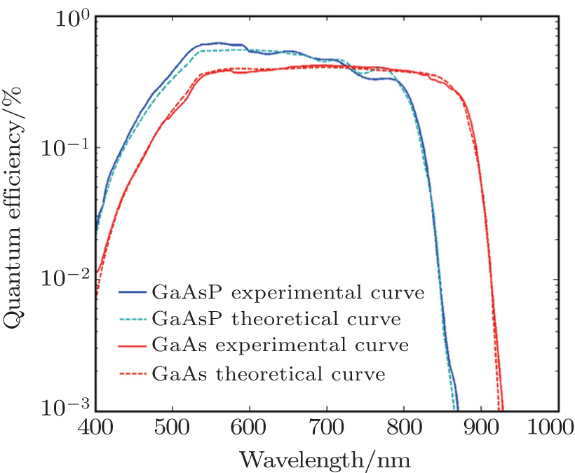
Fig. 6. Experimental and theoretical quantum efficiency curves of t-mode GaAsP and GaAs cathode samples.

From Fig. 6, it is seen that the inconsistency between experimental and theoretical quantum efficiency in the shortwave region for the GaAsP sample is ascribed to the improper absorption coefficient of the window-layer. According to Table 2, we find that the electron diffusion length and back interface recombination velocity of the GaAsP sample are nearly the same as those of the GaAs sample, which indicates that the crystalline quality of the grown cathode material, whether GaAsP- or GaAs-based sample, can meet the requirements. From Table 2, we can also find that the surface electron escape probability of the GaAsP sample is larger than that of the GaAs sample, which is similar to the experimental results observed by Escher and Antypas.[16]

Table 2.

Fitted performance parameters of t-mode GaAsP and GaAs cathode samples.

.

With an attempt to clarify the difference in surface electron escape probability between GaAsP and GaAs photocathodes, we should carry on an investigation into the inner band structure and surface barrier, which is shown in Fig. 7. The surface barrier profile based on the double dipole model comprises two approximately straight lines with different slopes, namely barriers I and II,[26] which are related to the Cs–O activation layer. As shown in Fig. 7, the high-energy photoelectrons excited by the shortwave photons near the back interface would relax into the Γ conduction-band minimum and preferentially traverse barrier II, while the low-energy photoelectrons excited by the longwave photons near the surface would consequently traverse barrier I without experiencing a thorough relaxation. As is well known, the profiles of barriers I and II would play a crucial role in surface electron escape.[20] On the one hand, for the small-bandgap GaAs sample, the longwave photoelectrons would become easier to escape to a vacuum because of the narrower barrier I. Besides, the larger red-NIR absorption in the thicker GaAs photocathode can also contribute to the number of longwave photoelectrons. On the other hand, for the large-bandgap GaAsP sample with a small electron affinity, the shortwave photoelectrons would escape to a vacuum more easily because of the narrower barrier II, while part of shortwave photoelectrons would possibly penetrate barrier I for the GaAs sample. Compared with barrier II, barrier I is more difficult to pass through for photoelectrons. Therefore, there are higher quantum efficiencies respectively in the blue–green waveband for the GaAsP photocathode and in the red-NIR waveband for the GaAs photocathode.

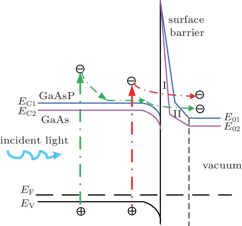
Fig. 7. Schematic band structures and surface barriers of the GaAsP and GaAs photocathode. EV is the valence band maximum, EF is the Fermi level, EC1 and EC2 are the conduction-band minima of GaAsP and GaAs respectively, and E01 and E02 are the vacuum levels of GaAsP and GaAs respectively.
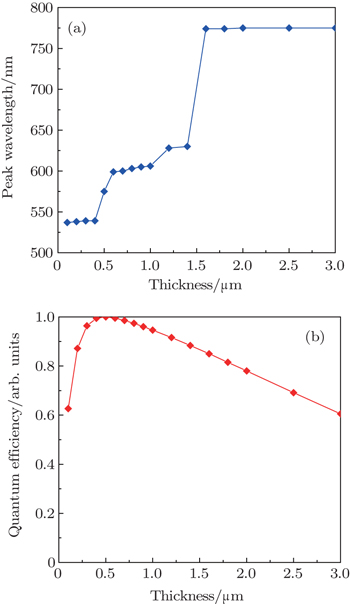
Fig. 8. Theoretical changes of (a) peak wavelength and quantum efficiency at 532 nm with emission-layer thickness.

In order to obtain the optimum thickness of the GaAs0.9P0.1 emission-layer for better blue–green response, we investigate the effects of emission-layer thickness on peak wavelength and quantum efficiency at 532 nm, respectively, and the simulation results are shown in Fig. 8. From Fig. 8(a), we can see that when the emission-layer thickness is within 0.6 μm, the peak wavelength can be in the blue–green waveband. Furthermore, it can be found from Fig. 8(b) that the quantum efficiency at 532 nm can reach its maximum when the emission-layer thickness ranges from 0.4 μm to 0.6 μmm. To sum up, the optimum thickness of the emission-layer is in a range of 0.4 μm–0.6 μm which would result in a better blue–green response, especially for the underwater range-gated imaging based on 532-nm-laser illumination.

4. Conclusions

In the present article, we have fabricated an 18-mm-diameter vacuum image tube incorporating the t-mode Al0.7Ga0.3As0.9P0.1/GaAs0.9P0.1 photocathode grown by MBE. A comparison of photoelectric property, spectral characteristic and performance parameter between the t-mode GaAsP-based and blue-extended GaAs-based photocathodes shows that the t-mode GaAsP-based photocathode achieves better absorption, higher quantum efficiency and narrower spectrum range in the blue–green waveband. Besides, the quantum efficiency of the t-mode GaAsP-based photocathode reaches as high as 59% at 532 nm, which is nearly twice that of the t-mode GaAs-based one. The simulation results show that the optimum thickness of the emission-layer is in a range of 0.4 μ–0.6 μm, which is advantageous to range-gated imaging underwater. This work could provide a reference for further improving the performance of the t-mode GaAsP-based photocathode for better blue–green response.

Reference
1Edgecumbe J PAebi V WDavis G A 1992 Proc. SPIE 1655 204
2Kirschner JOepen H PIbach H1983Appl. Phys. A30177
3Mirzoyan RFerenc DLorenz E 2000 Nucl. Instrum. Methods Phys. Res. 442 140
4Contarino V MMolchanov P AAsmolova O V 2005 Proc. SPIE 5656 156
5Bazarov I VDunham B MLi YLiu XOuzounov D GSinclair C KHannon FMiyajima T 2008 J. Appl. Phys. 103 054901
6Maruyama TLuh D ABrachmann AClendenin J EGarwin E LHarvey SPrepost RMoy A M 2004 Appl. Phys. Lett. 85 2640
7Jin XOzdol BYamamoto MMano AYamamoto NTakeda Y 2014 Appl. Phys. Lett. 105 203509
8Hayashida MNinkovic JHose JHsu C CMirzoyanTeshima M 2007 Nucl. Instrum. Methods Phys. Res. 572 456
9Hayashida MMirzoyan RTeshima M 2006 Nucl. Instrum. Methods Phys. Res. 567 180
10Ohnuki TMichalet XTripathi AWeiss SArisaka K 2006 Proc. SPIE 6092 60920P
11Saito YMishima KMatsubayashi MLim I CCha J ESim C H 2005 Nucl. Instrum. Methods Phys. Res. 542 309
12Giudicotti LPasqualotto RAlfier ABeurskens M N AKempenaars MFlanagan J CWalsh M JBalboa I 2011 Fusion Eng. Des. 86 198
13LaRue RHttps://www.sbir.gov/sbirsearch/detail/201796 [2007]
14Antypas G AEdgecumbe J 1975 Appl. Phys. Lett. 26 371
15Nahory R EPollack M AJohnston W DBarns R L 1978 Appl. Phys. Lett. 33 659
16Escher J SAntypas G A 1977 Appl. Phys. Lett. 30 314
17Seredin P VLenshin A SGlotov A VArsentyev I NVinokurov D ATarasov I SPrutskij TLeiste HRinke M 2014 Semiconductors 48 1094
18Jiao G CHu C LLiu JQian Y S 2015 Appl. Opt. 54 8473
19Zhang Y JNiu JZhao JXiong Y JRen LChang B KQian Y S 2011 Chin. Phys. 20 118501
20Zhang Y JNiu JZou J JChang B KXiong Y J 2010 Appl. Opt. 49 3935
21Sinor T WEstrera J PPhillips D LRector M K 1995 Proc. SPIE 2551 130
22Https://www.hamamatsu.com/resources/pdf/etd/C9016 TAPP1046E.pdf [2009]
23Zhang Y JNiu JZhao J JChang B K 2011 Acta Phys. Sin. 60 067301 (in Chinese)
24Aspnes D EKelso S MLogan R ABhat R 1986 J. Appl. Phys. 60 754
25Cetin S SKinaci BAsar TKars IOzturk M KMammadov T SOzcelik S 2010 Surf. Interface Anal. 42 1252
26Su C YSpicer W ELindau I 1983 J. Appl. Phys. 54 1413