


Subsurface defect characterization and laser-induced damage performance of fused silica optics polished with colloidal silica and ceria
[He Xiang, Wang Gang, Zhao Heng, Ma Ping†,  ]
]
]
|
|


† Corresponding author. E-mail:
This paper mainly focuses on the influence of colloidal silica polishing on the damage performance of fused silica optics. In this paper, nanometer sized colloidal silica and micron sized ceria are used to polish fused silica optics. The colloidal silica polished samples and ceria polished samples exhibit that the root-mean-squared (RMS) average surface roughness values are 0.7 nm and 1.0 nm, respectively. The subsurface defects and damage performance of the polished optics are analyzed and discussed. It is revealed that colloidal silica polishing will introduce much fewer absorptive contaminant elements and subsurface damages especially no trailing indentation fracture. The 355-nm laser damage test reveals that each of the fused silica samples polished with colloidal silica has a much higher damage threshold and lower damage density than ceria polished samples. Colloidal silica polishing is potential in manufacturing high power laser optics.
The laser-induced damage of fused silica optics used in large high power laser facilities has been an extensive research subject. Pure fused silica as one of the most important optical materials has a wide bandgap and very high intrinsic laser-induced damage threshold.[1] However, even the highest quality optical components have lots of manufacturing (cutting, grinding or polishing) induced subsurface defects which restrict the damage resistance.[2,3] At present, ceria particles are commonly used to polish silicon-oxygen based glass for their high polish rate. But ceria polishing also has some disadvantages such as broad size distribution and irregular shapes of the particles, coagulation of the slurry, and introduction of contaminants of several metal elements.[4] Therefore, ceria polishing would possibly induce an absorptive contaminant (such as Ce and Fe) and subsurface fractures,[5] which is responsible for triggering the surface damage of fused silica optics.[6–9] Some researchers also have investigated the influences of different polishing slurries such as ceria, zirconia and alumina on the damage performance.[7,10–15] They showed that the polishing slurries used in chemical mechanical polishing have great influences on the subsurface defect distribution and damage performance of the polished optics. Compared with ceria particles, nanometer sized colloidal silica particles are uniform spheres and have a narrow size distribution. Colloidal silica polishing is more appropriate for obtaining a high quality surface.[4] However, using colloidal silica polishing instead of ceria polishing to achieve a damage-free fused silica surface for improving the 355-nm laser damage performance has been rarely investigated.
In the present paper, commercially available micron sized ceria and nanometer sized colloidal silica are used to polish fused silica optics. Then, the polishing induced subsurface defects and laser-induced damage performance of the polished samples are analyzed and discussed. The contaminant elements in the redeposition layers are analyzed by time-of-flight secondary ion mass spectrometry (TOF-SIMS). The combination of HF etching and differential interference contrast (DIC) microscopy is used to detect the subsurface damages. The results reveal that using colloidal silica polishing instead of ceria polishing would induce much fewer subsurface defects and substantially improve the damage resistance of fused silica optics.
Six commercially available precisely polished UV-grade fused silica samples, each with 50 mm in diameter and 5 mm in thickness, (labeled as A1, A2, A3, B1, B2, and B3) were manufactured by loose abrasive grinding and polishing. The grinding processes (by using 14-μm SiC and 5-μm SiC sequentially) were the same for all of the samples by using a copper pad. Samples A1, A2, and A3 were polished with ceria while samples B1, B2, and B3 were polished with colloidal silica. All of the polishing processes were performed by a single side polisher with a polishing cloth instead of pitch, in the same conditions such as pressure (190 g/cm2) and rotation speed (30 rpm for pad; 30 rpm for sample). Note that the material removal rate of colloidal silica polishing is much lower than that of ceria polishing (∼ 2 μm/h). Thus, much more time was taken to completely eliminate the residual subsurface damages induced by the grinding process in polishing samples B1, B2, and B3. In order to avoid the cross contamination in the polishing process, a fresh polishing cloth was used to polish samples B1, B2, and B3 after the preparation of samples A1, A2, and A3. The detailed sample preparation methods are given in Table
| Table 1. Sample preparation methods. . |
The size distributions of the two commercially available polishing slurries were measured by a Zetasizer Nano ZS nano-particle analyzer. The peak particle sizes of colloidal silica (Unicol 50) and ceria (Hastilite 919) are 70 nm and 950 nm, respectively. The particle size distribution of colloidal silica is in a range from 30 nm to 200 nm while that of ceria is from 300 to 1800 nm. Colloidal silica slurry has a much narrower size distribution and smaller average size than ceria. The surface roughness of each sample was measured with a white light interferometer. The depth profiles of the contaminant elements in the redeposition layers were detected by a Model 2100 Trift II TOF-SIMS.
A tripled Nd:YAG laser at a wavelength of 355 nm was used in our laser-induced damage test equipment. The pulse is a single longitudinal mode with a full-width at half-maximum (FWHM) value of about 5 ns. During the test, the beam was focused on the exit surface to provide a near-Gaussian beam with a diameter of about 0.7 mm at 1/e2 of maximum intensity. Fluence fluctuations have a standard deviation of about 10%. The on-line microscope has a resolution of about 10 μm. The damage threshold was obtained by using the standard “1-on-1” test mode. A raster scan damage test was used to detect the damage density and the scan area is about 4 cm2. Here the damage density means the number of catastrophic damage craters per square centimeter in the raster scan damage test area at a certain laser fluence, say, 12 J/cm2. The damage morphologies were acquired by a Leica DM4000M optical microscope.
The subsurface damages are generally covered by the redeposition layer after the polishing process and are hard to detect. Since HF etching could expose and widen the invisible subsurface damages, and DIC images are much more sensitive to small pits and shallow scratches than normal bright field images.[16] The HF etching and DIC images could be combined to analyze the subsurface damages of polished surfaces. After the previous measurements, both sides for each of all samples were etched 1 μm in HF based acid. Then the DIC images of the HF etched samples were acquired to detect the subsurface damages via a Leica DM4000M optical microscope equipped with a DIC module. To obtain the statistical distribution of the subsurface damages in full size, more than ten DIC images (650 μm 480 μm) of each HF etched sample, evenly spaced along the diameter, were recorded.
Figure
 | Fig. 1. The surface roughness values of samples: (a) A1, (b) A2, (c) A3, (d) B1, (e) B2, and (f) B3. |
The SIMS tests reveal that the main contaminant elements in all samples consist of Ce, Fe, Al, K, and Na. All of the contaminant elements show rapid decrease and disappear at a depth of 100 nm for all samples. The depth profile data are normalized with the silicon ion number (counts 104) as a standard for comparison. The cumulated quantities of the elements in the 100-nm redeposition layers for all the samples are presented in Table
| Table 2. Cumulated quantities of elements in the redeposition layers of each of all the samples. . |
Figure
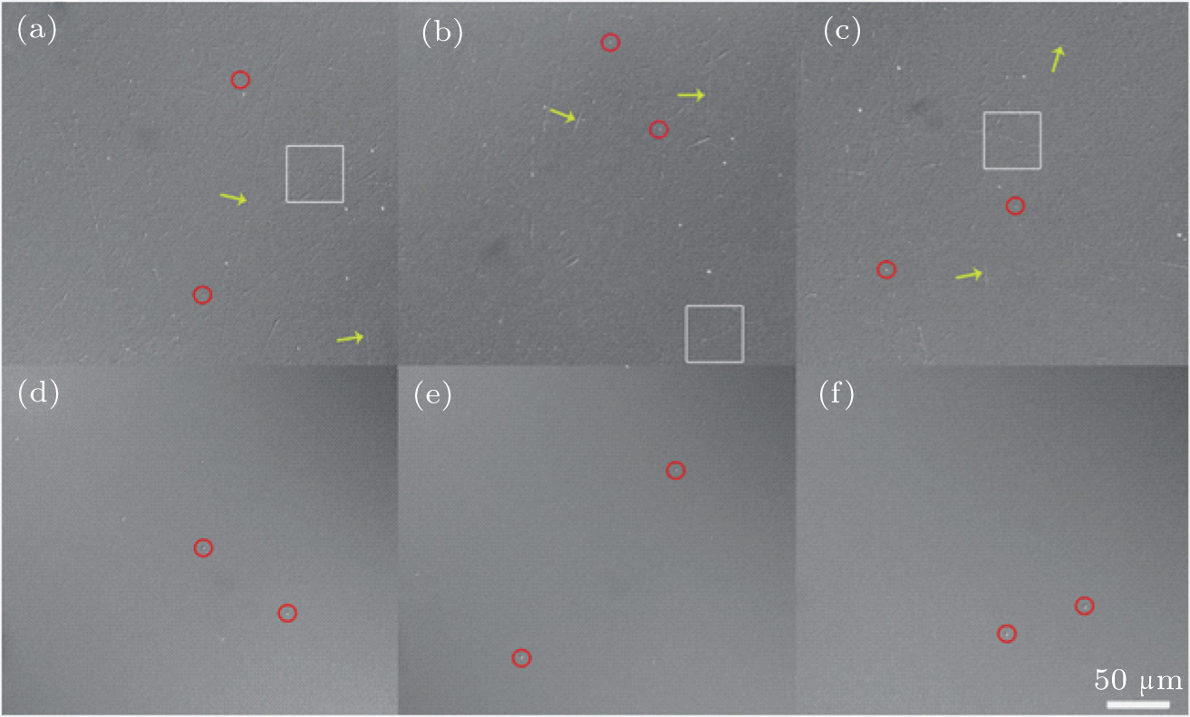 | Fig. 2. The DIC images of the HF etched surfaces of samples (a) A1, (b) A2, (c) A3, (d) B1, (e) B2, and (f) B3. Different kinds of subsurface damages are marked by different symbols in each panel: red circle for polishing dot, green arrow for continuous polishing scratch, and white arrow for trailing indentation fracture. |
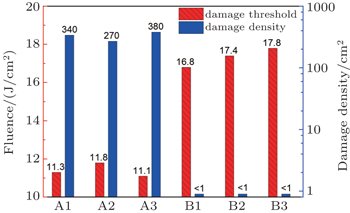
Figure
 | Fig. 3. The 355-nm laser-induced damage threshold (red bias column) and damage density (blue blank column) at a fluence of 12 J/cm2 for the samples manufactured by different procedures. |
Recent studies suggested that two kinds of near surface defects are primarily responsible for triggering the surface damage of fused silica optics exposed to 355-nm ultraviolet wavelength in a low fluence range.[6] One is the highly absorptive contaminant (such as Ce and Fe) coming from chemical mechanical polishing, and the other is the subsurface fracture (or subsurface damage) produced by grinding or polishing of brittle materials. These dangerous near surface defects can modulate light intensity, absorb UV laser fluence and finally lead to plasma explosion (or surface damage) at extremely low laser fluence (far lower than the intrinsic damage threshold of fused silica). Liu et al. have revealed that the content of Ce contaminant has a great influence on the damage threshold.[20] Camp et al. have found that bigger, deeper subsurface damages would reduce the damage threshold more.[11] The laser damage initiation is strongly correlated with fracture as indicated in Refs. [12]–[23]. In the ceria polishing process, the larger ceria particles will create many subsurface damages especially the fracture related trailing indentation fractures (Figs.
The initial laser-induced damage morphologies of all samples are illustrated in Fig.
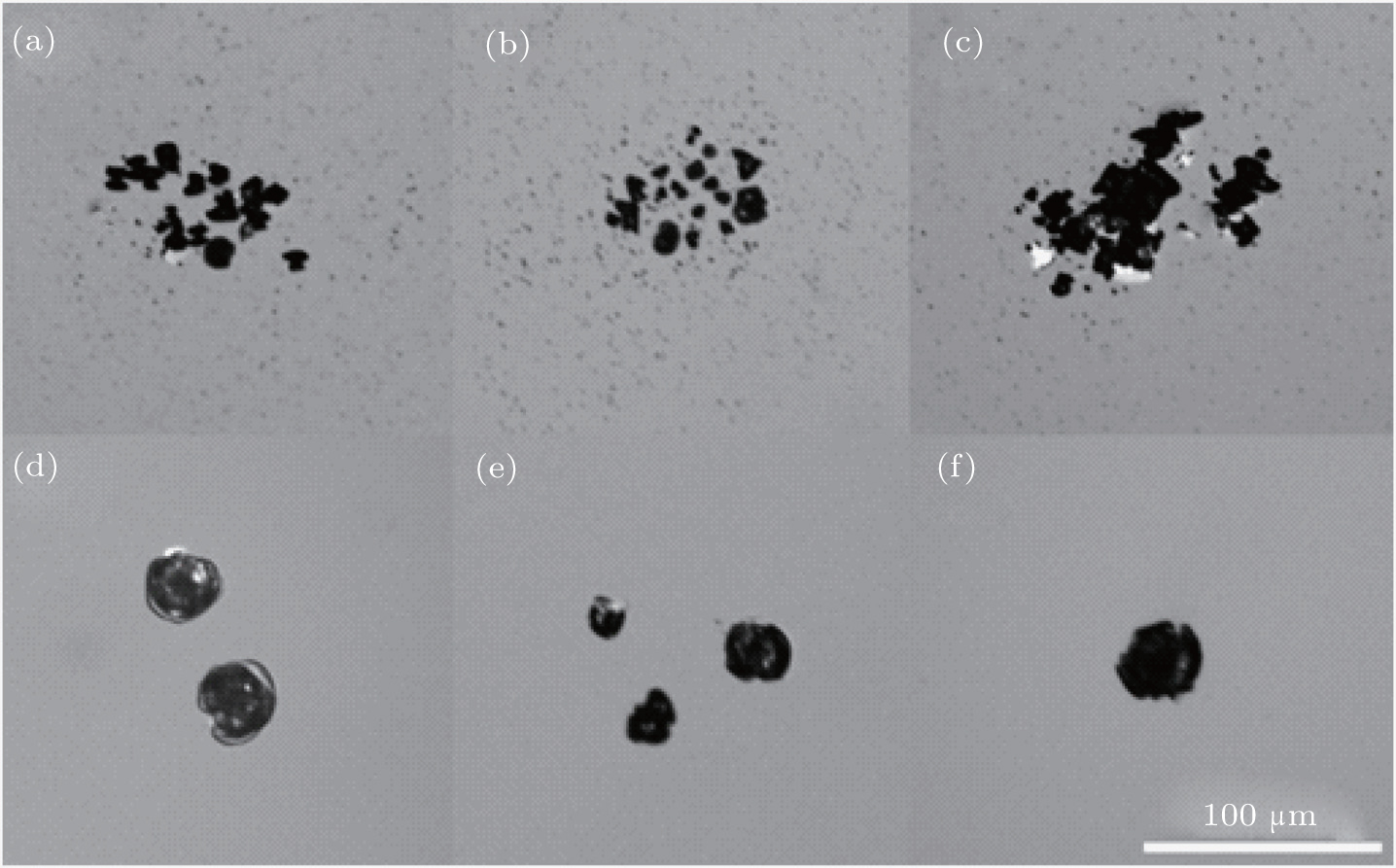 | Fig. 4. Initial laser-induced damage morphologies (captured in 1-on-1 damage test, 5-ns pulse) of samples (a) A1, (b) A2, and (c) A3 at a laser fluence of 12 J/cm2, (d) B1, (e) B2, and (f) B3 at a fluence of 17 J/cm2. |
In this paper, nanometer sized colloidal silica and micron sized ceria polishing slurries are used to polish fused silica samples. The surface roughness, subsurface defect characterization and laser damage performance of each polished sample are analyzed and discussed. We can conclude that the contaminant elements in the redeposition layers and the surface roughness are mainly determined by the final polishing process. The colloidal silica polished samples present an average surface roughness value of 0.7 nm while the ceria polished samples have an average surface roughness value of 1.0 nm. Colloidal silica polishing would introduce much fewer absorptive contaminant elements (Ce, Fe) than ceria polishing. In addition, colloidal silica polishing introduces much fewer subsurface damages especially no trailing indentation fracture. The 355-nm laser damage tests prove that colloidal silica polishing could greatly improve the damage resistance of fused silica optics than ceria polishing. Colloidal silica polishing can potentially be used in manufacturing high power laser optics.
| 1 | |
| 2 | |
| 3 | |
| 4 | |
| 5 | |
| 6 | |
| 7 | |
| 8 | |
| 9 | |
| 10 | |
| 11 | |
| 12 | |
| 13 | |
| 14 | |
| 15 | |
| 16 | |
| 17 | |
| 18 | |
| 19 | |
| 20 | |
| 21 | |
| 22 | |
| 23 |