
Numerical simulation of the magnetoresistance effect controlled by electric field in p–n junction
[Yang Pan, Chen Wen-Jie, Wang Jiao, Yan Zhao-Wen, Qiao Jian-Li, Xiao Tong, Wang Xin, Pang Zheng-Peng, Yang Jian-Hong†,  ]
]
]
|
|


† Corresponding author. E-mail:
The magnetoresistance effect of a p–n junction under an electric field which is introduced by the gate voltage at room temperature is investigated by simulation. As auxiliary models, the Lombardi CVT model and carrier generation-recombination model are introduced into a drift-diffusion transport model and carrier continuity equations. All the equations are discretized by the finite-difference method and the box integration method and then solved by Newton iteration. Taking advantage of those models and methods, an abrupt junction with uniform doping is studied systematically, and the magnetoresistance as a function of doping concentration, SiO2 thickness and geometrical size is also investigated. The simulation results show that the magnetoresistance (MR) can be controlled substantially by the gate and is dependent on the polarity of the magnetic field.
In view of the physical interest and potential applications, magnetoresistance (MR) effects have attracted a lot of theoretical and experimental attention. MR effects can be achieved by using non-magnetic materials such as doped silicon,[1] GaAs,[2] and magnetic materials.[3,4] However, compared with magnetic material, non-magnetic material has a large MR ratio and the resistivity increases approximately linearly with the external magnetic field, which makes the non-magnetic material more attractive to random access memory, ultrasensitive magnetic field sensors,[5] logic devices,[6,7] etc. By virtue of long spin coherence[8,9] and compatibility with the current CMOS technology, silicon is a promising material for investigating the magnetoresistance effect.
Many researches based on doped silicon have been carried out to explore the effect. Michael et al. have reported that the large positive magnetoresistance effect can be induced by breaking the quasi-neutrality of the space-charge effect.[10] While another mechanism was also proposed, i.e., the magnetoresistive effect can be achieved by shrinking the acceptor wave functions in the direction perpendicular to the magnetic field.[11] Meanwhile, it can also be achieved by the process of impact ionization[12] which is controlled by magnetic field.
However, a few methods are put forward to regulate MR when the magnetic field is fixed. Though varying the geometrical size[13] can achieve it, it is inconvenient for practical applications. In the present work, the magnetoresistance effect of the p–n junction induced by the space-charge effect under an electric field is studied by simulation. The results show that a wide range of magnetoresistance can be controlled, which implies that it is a more potential method to adjust magnetoresistance by using the electric field which is introduced by gate voltage.
Classical p–n theories proposed by Shockley[14] are basic to analyse the properties of the p–n junction. This theory consists of a set of fundamental equations, which need to be modified slightly when they are used to simulate the properties of p–n under the external magnetic field and electric field.


Equations (


To obtain accurate results, the Lombardi CVT Model,[17] which contains the effect of a transverse field, doping- and temperature-dependent carrier mobility, is used. In this model, the mobility is given by three components that are composed according to the Matthiessen rule:

On the right-hand side of Eq. (
For numerical simulation of a semiconductor device, the carrier generation-recombination is the crucial process that must be considered. In this paper, Shockley–Read–Hall recombination[18] and Auger recombination[19] within the bulk of the semiconductor are adopted.


During numerical simulation, several boundary conditions (ohmic contacts, insulated contacts, Neumann boundaries) must be considered. To implement ohmic contacts, Dirichlet boundary conditions, where surface potential, electron concentration and hole concentrations are fixed, are taken into account. In the oxide region, the zero normal current condition
To discretize those equations, the finite-difference method and the box integration method are used in order to solve them in an appropriate mesh. After discretization, the Newton iteration is used to solve the partial differential equations. The SGFramework,[21] a highly flexible partial differential equations solver, is introduced.
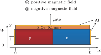
The structure simulated is shown in Fig.
 | Fig. 1. Schematic diagram of the p–n junction device, where the length L is 10 μm and width W is 5 μm. |
| Table 1. Simulation parameters. . |
Figure
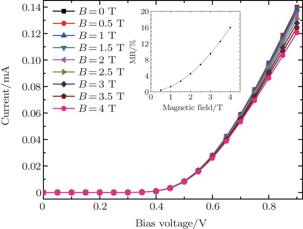 | Fig. 2. I–V characteristics of the p–n junction at T = 300 K for various magnetic fields. The inset demonstrates MR at Vbias = 0.9 V. |
Figure
 | Fig. 3. Spatial distributions of space-charge region induced by the magnetic field (the colour has no special implication) for the cases (a) without magnetic field and (b) with positive magnetic field. |
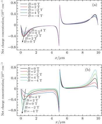
Figures
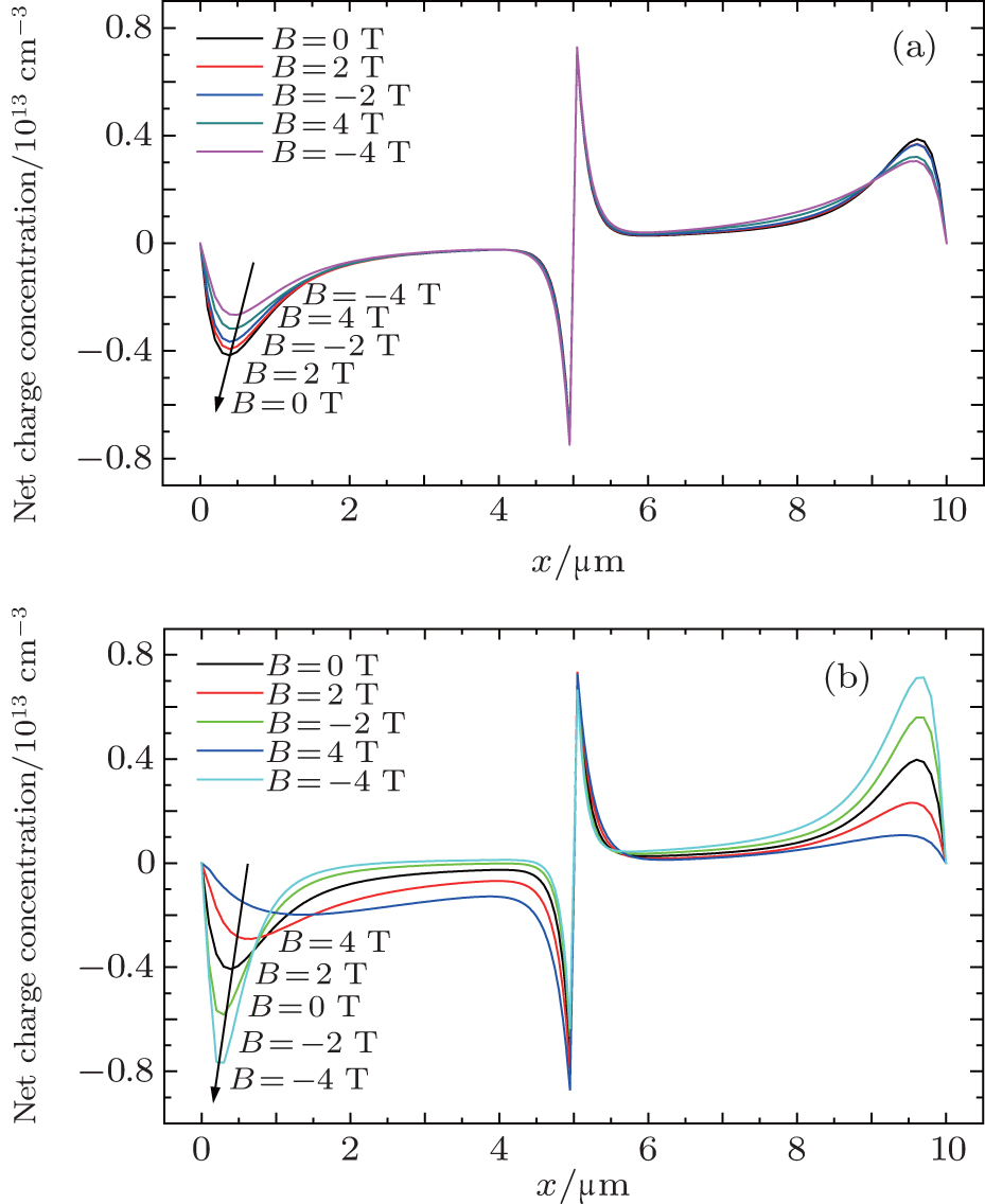 | Fig. 4. Net charge concentrations for various magnetic fields at Vbias = 0.9 V, y = 2.5 μm (a) and 0.3 μm (b). |
In order to discuss the magnetoresistance effect of the p–n junction under an electric field clearly, here, the MR ratio is modified into M1(%) = [R(B,Vgate) − R(0)]/R(0) × 100%, where R(0) and R(B,Vgate) are the resistance (V/I) at zero applied magnetic field and that at applied magnetic field B and gate voltage Vgate. MR1 can also be given by MR1 = MR + ΔRE/R0 + f (B,E), where ΔRE = R(B = 0 T,Vgate) − R(B = 0 T,Vgate = 0 V) is the resistance variation (B = 0 T). MR and ΔRE/R0 are the resistance variation ratios without gate voltage and without magnetic field respectively, f (B,E) is an interaction term induced by the interaction between magnetic field and gate voltage.
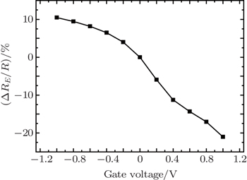
At the zero-magnetic field, the resistance increases with an increase of negative gate voltage applied and decreases with the increase of positive gate voltage. The resistance variation ratio (ΔRE/R0) without magnetic field is shown in Fig.
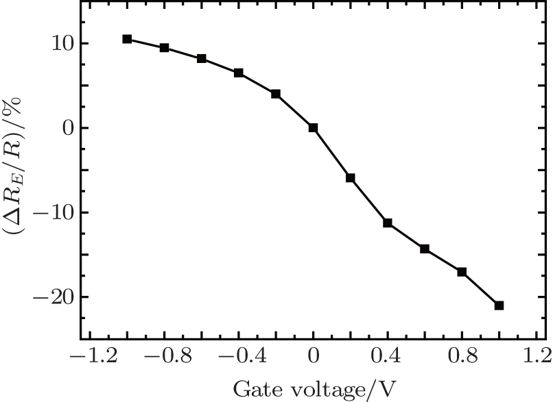 | Fig. 5. Variation of resistance ratio with gate voltage at B = 0 T and Vbias = 0.9 V. |
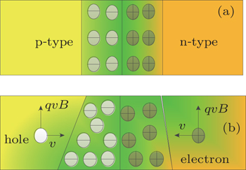
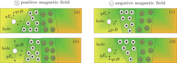
To explore the variation of f (B,E), the force analysis of hole under magnetic field and gate voltage is shown in Fig.
 | Fig. 6. The spatial distributions of space-charge region with different conditions: (a) with positive magnetic field and negative gate voltage; (b) with positive magnetic field and gate voltage; (c) with negative magnetic field and negative gate voltage; (d) with negative magnetic field and positive gate voltage. The qvB is the Lorentz force and qEe is the electric field force. |
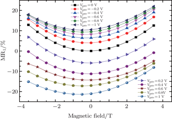
On the basis of the above discussion, the results shown in Fig.
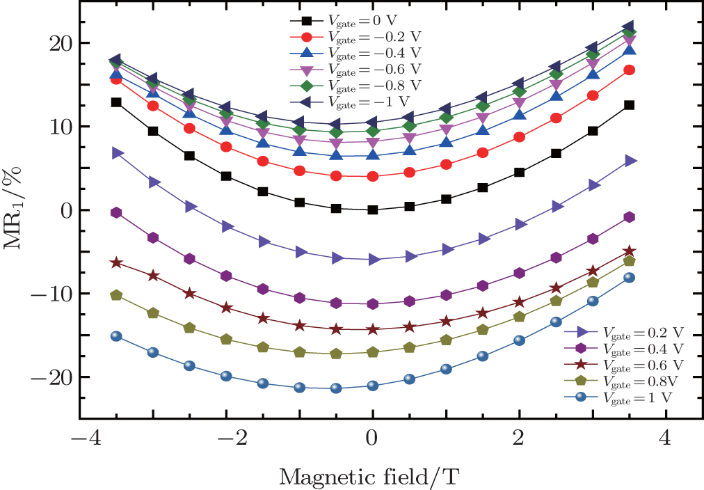 | Fig. 7. Variations of MR1 with magnetic field for various gate voltages at a bias voltage of 0.9 V. |
In addition, it can also be noted that the MR is about 0.396% with a magnetic field of 0.5 T and an applied bias voltage of 0.9 V, while an 11.107% magnetoresistance ratio is achieved with a negative gate voltage of −1 V at the same bias voltage. The MR is enlarged substantially due to the contribution of ΔRE/R0 (f (B,E) is small.) However, the distinction of the magnetoresistance curve between various negative gate voltages disappears with magnetic field increasing and gate voltage decreasing. It can be explained by the fact that the ΔRE/R0 tends to be saturated which is shown in Fig.
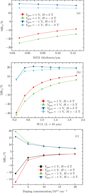
Figure
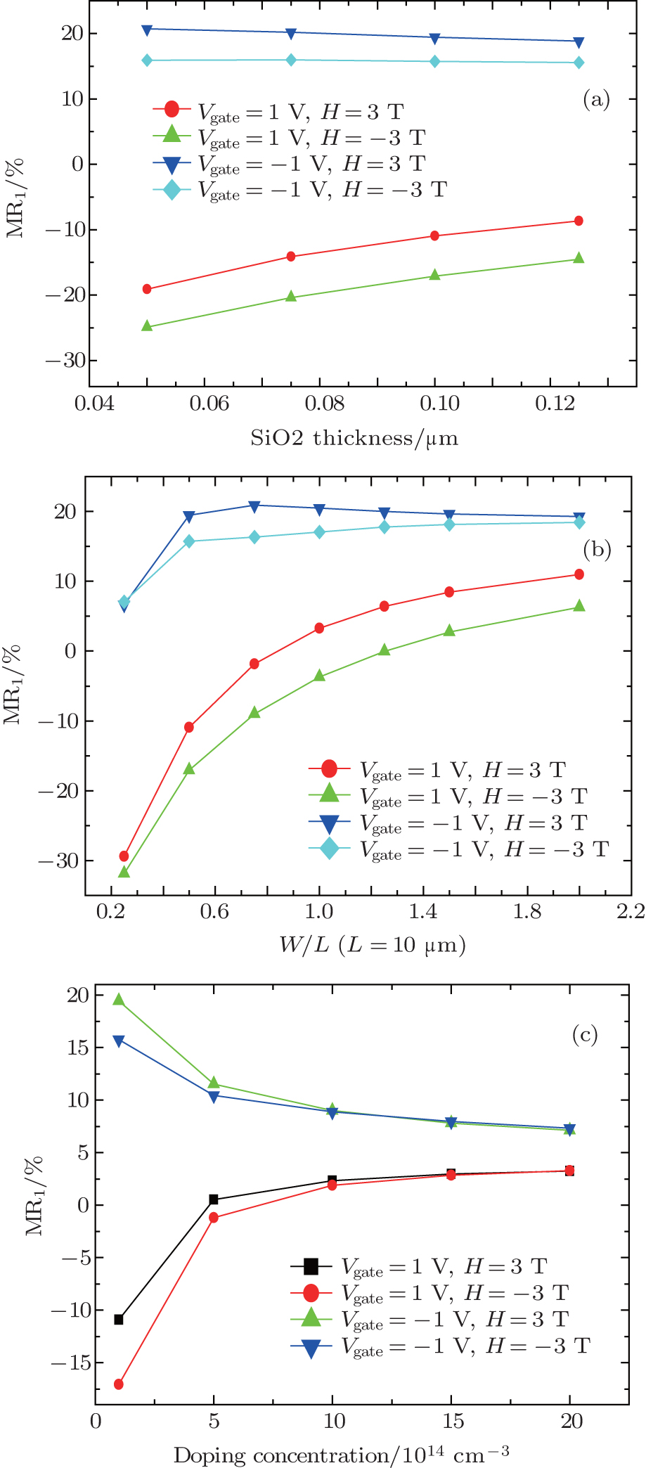 | Fig. 8. Variations of MR1 with (a) SiO2 thickness with W = 5 μm, L = 10 μm, and NA = ND = 1×1014 cm−3, (b) W/L with SiO2 thickness d = 0.1 μm, L = 10 μm, and NA = ND = 1×1014 cm−3, (c) doping concentration (NA = ND) with W = 5 μm, L = 10 μm, and NA = ND = 1×1014 cm−3. A bias voltage of 0.9 V is applied at T = 300 K under conditions in panels (a), (b), and (c). |
In this paper, the magnetoresistance effect of the p–n junction under an electric field at room temperature is simulated. The results indicate that it is a useful method to control magnetoresistance by gate voltage. A larger MR can be achieved by negative gate voltage, and it can also be compensated by positive gate voltage. Meanwhile, MR is dependent on the polarity of magnetic field when gate voltage is applied. Furthermore, the doping concentration, SiO2 thickness and p–n junction size are also investigated. The results will promote the applications of silicon-based magnetoresistance devices such as a reconfigurable logic device based on magnetoresistance, access memories, and so on.
| 1 | |
| 2 | |
| 3 | |
| 4 | |
| 5 | |
| 6 | |
| 7 | |
| 8 | |
| 9 | |
| 10 | |
| 11 | |
| 12 | |
| 13 | |
| 14 | |
| 15 | |
| 16 | |
| 17 | |
| 18 | |
| 19 | |
| 20 | |
| 21 |