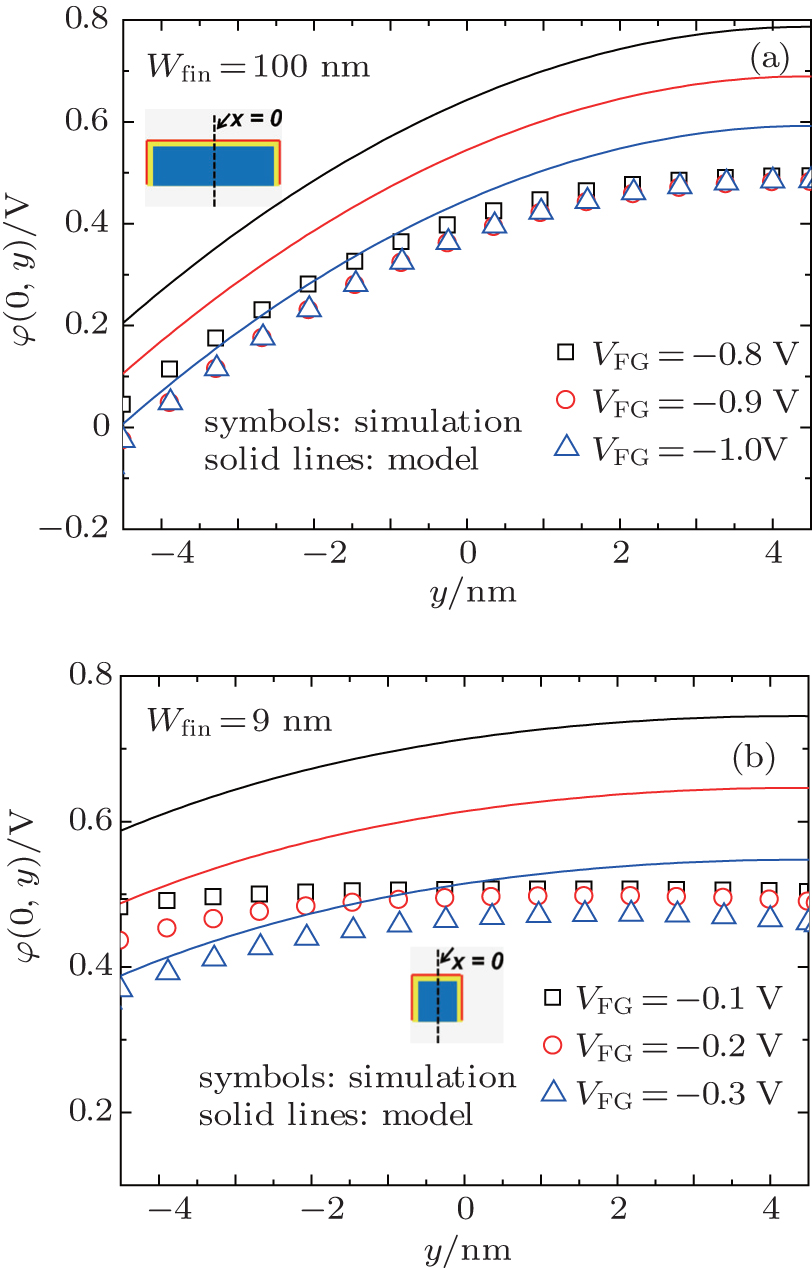
An analytical model for nanowire junctionless SOI FinFETs with considering three-dimensional coupling effect
Liu Fan-Yu1, †,  , Liu Heng-Zhu1, Liu Bi-Wei1, Guo Yu-Feng2
, Liu Heng-Zhu1, Liu Bi-Wei1, Guo Yu-Feng2 Potential profiles in partially-depleted region along