An analytical model for nanowire junctionless SOI FinFETs with considering three-dimensional coupling effect
Liu Fan-Yu1, †, , Liu Heng-Zhu1, Liu Bi-Wei1, Guo Yu-Feng2
School of Computer, National University of Defense Technology, Changsha 410073, China
Electronic Science and Engineering, Nanjing University of Posts and Telecommunications, Nanjing 201131, China


† Corresponding author. E-mail: liufanyu986412@hotmail.com

Project supported by the Research Program of the National University of Defense Technology (Grant No. JC 13-06-04).

Abstract
Abstract

In this paper, the three-dimensional (3D) coupling effect is discussed for nanowire junctionless silicon-on-insulator (SOI) FinFETs. With fin width decreasing from 100 nm to 7 nm, the electric field induced by the lateral gates increases and therefore the influence of back gate on the threshold voltage weakens. For a narrow and tall fin, the lateral gates mainly control the channel and therefore the effect of back gate decreases. A simple two-dimensional (2D) potential model is proposed for the subthreshold region of junctionless SOI FinFET. TCAD simulations validate our model. It can be used to extract the threshold voltage and doping concentration. In addition, the tuning of back gate on the threshold voltage can be predicted.

1. Introduction

Since their invention by J-P. Colinge, junctionless (JL) transistors have been a compelling candidate for ultra-scaled devices due to their excellent electrostatic gate control and simplified junction engineering.[1] These transistors have shown the promising applications in the field of analog/RF,[2] logic[3] and sensing circuits.[4] JL MOSFETs are usually designed with heavily doped silicon films (∼ 1019 cm−3) in order to achieve enough drain current. Owing to the high doping concentration of the channel, the carrier transport in a JL transistor relies on volume conduction instead of the conventional surface inversion in MOSFET. This device is switched off by fully depleting its heavily doped channel. Thus, the geometry of the channel must be small enough to permit the full depletion at a desired gate voltage. The junctionless transistor can operate in three modes: full depletion, partial depletion, and surface accumulation. The threshold voltage and flat-band voltage are the key identifiers to distinguish the three modes.

In classical inversion-mode FD SOI MOSFET, the operation of the transistor is governed by both front and back channels. This phenomenon is well known as the coupling effect between front and back gates, which has been demonstrated to have a strong influence on the threshold voltage and mobility.[57] However, most studies of the coupling effect involve the inversion-mode SOI MOSFETs with undoped or low-doped channel. There are few reports on the coupling effect in the JL transistor with a heavily doped channel. Owing to the small cross-section of the channel in the JL transistor, the coupling effect is expected to happen as in the inversion-mode SOI MOSFETs.[8,9]

On the other hand, the junctionless SOI FinFET with multiple gates has been fabricated due to its novel performance.[10,11] In the JL SOI FinFET, we must consider the effect of the lateral electric field between the two lateral gates. This lateral electric field which makes the difference between planar and FinFETs enhances the coupling effect. The enhanced coupling effect will lead to the difficulties in determining the threshold voltage, which reflects the full depletion of the doped channel. Several models based on the approximate solution of the Poisson equation have been proposed: a one-dimensional (1D) model for double-gate JL devices,[1214] a 1D potential model in the full depletion region for double-gate JL transistors,[15] a 2D surface-potential-based current model for triple-gate transistors,[16] etc. While 2D models are too complicated to be used for parameter extraction, a 1D model does not consider the coupling effect between the gates.[17] Therefore, a simple model including the coupling effect between gates is imperative for parameter extraction in JL SOI FinFET.

In this paper, we will take the coupling effect into account in the modeling of JL SOI FinFET. We focus on the modeling of potential and the coupling effect in the subthreshold region (depletion region for JL transistor). Section 2 will show the evidence of coupling effects in JL SOI FinFETs. In Section 3, we will propose a 2D model for potential distribution in a subthreshold region. TCAD simulations are performed to validate our model. Based on this model, a simple and fast method to determine the threshold voltage is developed by considering the coupling effects, which will be explained in Section 4. In Section 5 we will draw some conclusions from the present study.

2. Coupling effect in junctionless SOI FinFET

Before the 2D analytical model with considering the coupling effect in JL SOI FinFETs, we will firstly show the simulated characteristics of JL SOI FinFETs. The coupling effects will be uncovered by comparing the influences of fin width, film thickness and backgate on the characteristic curves.
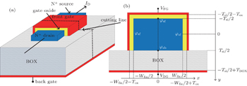
2.1. TCAD simulation set-up

Figure 1 shows the simulated structure for an n-channel JL SOI FinFET. The Si film thickness is 9 nm.[18] The thickness values of gate oxide and buried oxide (BOX) are respectively 1.2 nm and 145 nm.[18] The channel has a high arsenic doping concentration of ∼ 1019 cm−3.[18] In order to reduce the access resistance, the source and drain are heavily doped with arsenic (1020 cm−3). The back gate contact is directly placed on the bottom of buried oxide in order to omit the effect of substrate depletion. The gate length is fixed to be 200 nm to avoid the short-channel effect. The width of channel varies from 7 nm to 100 nm.

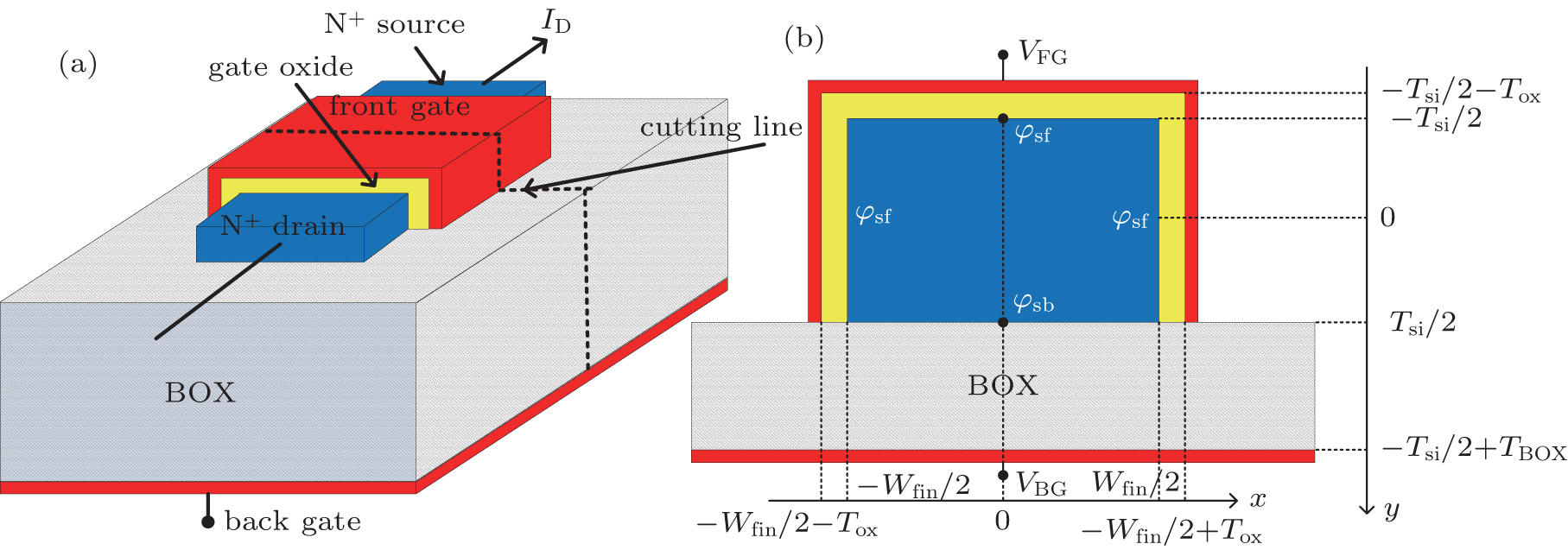
Fig. 1. (a) Schematic structure and (b) cross-section for simulated n-channel JL SOI FinFETs.

Synopsys Sentaurus TCAD is employed for all simulations.[19] Fermi-Dirac distribution is employed due to the heavily doped channel. The effect of doping, velocity saturation and the surface scattering are considered. The Shockley–Read–Hall recombination dependent on the doping level and Auger recombination are also included. The work-functions of the front and back gates are selected to make the flat-band voltages (VFBF and VFBB) equal zero. Both the front- and the back-gate leakages are neglected.[18] The drain is 0.05 V and the gate is swept from −1.5 V to +1.5 V. All the simulations are 3D simulations.

2.2. Simulated results
2.2.1. Characteristic curves

Figure 2 shows the plots of simulated drain current and transconductance versus front gate voltage (VFG) for JL SOI FinFETs with different fin widths. For VFG = 0 V (corresponding to flat-band), the drain current is significant due to volume conduction. At a higher front gate voltage, the drain current increases further as a result of an activated accumulation channel under the front gate. For VFG < 0 V, the current decreases until the channel is fully depleted (∼ −1.1 V for Wfin = 100 nm, where a sharp decrease of drain current is observed in the semi-logarithmic scale of Fig. 2(a)).

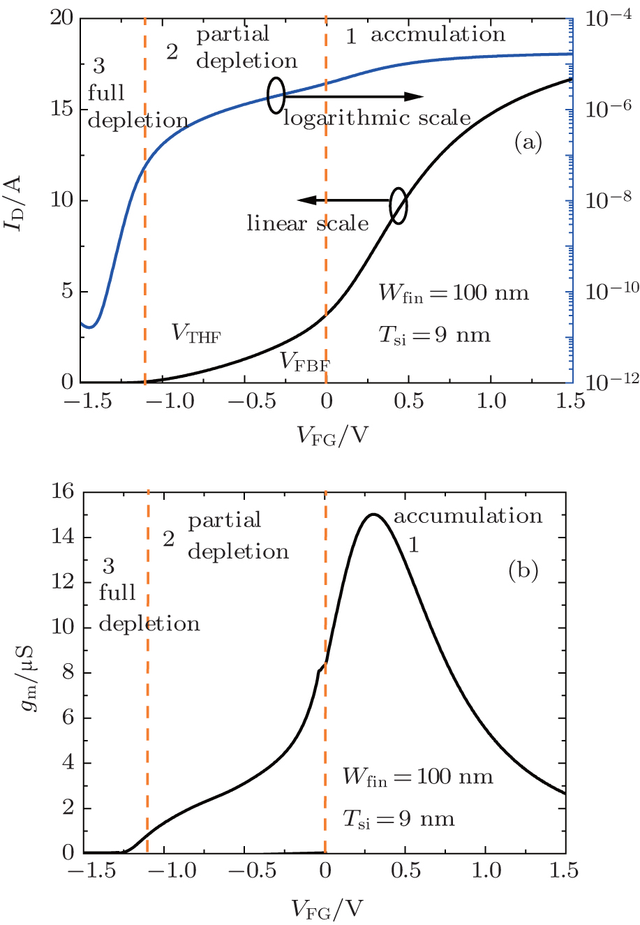
Fig. 2. (a) Simulated drain currents and (b) transconductance versus front gate voltage for wide JL SOI FinFETs. ND = 1019 cm−3, Tsi = 9 nm, VD = 0.05 V, and VBG = 0 V.

These modes of operation are also reflected by the contours of electron density in Fig. 3. For VFG = VFBF (input value is 0 V), the drain current equals the volume current (Fig. 3(a)). The junctionless transistor can work in three modes:

accumulation mode (VFG > VFBF), in which the drain current is the sum of volume current and accumulation current (Fig. 3(b));

partial depletion mode, in which the drain current comes from the volume conduction in the undepleted region (Fig. 3(c));

full depletion mode, in which the drain current decreases sharply with VFG (Fig. 3(d)).

Fig. 3. Electron density profiles (cm−3) for (a) only volume conduction, (b) accumulation, (c) partial depletion, and (d) full depletion. ND = 1019 cm−3, Tsi = 9 nm, VD = 0.05 V, and VBG = 0 V.
2.2.2. Effect of fin width and film thickness

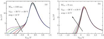
The effect of fin width on the transconductance curves gm(VFG) is shown in Fig. 4(a). For wide fin (Wfin = 100 nm), a plateau appears in the partially depleted region (−1.1 V < VFG < 0 V) due to the volume conduction. With the fin width decreasing, the gm plateau reduces until it disappears. This can be attributed to the enhanced control of lateral gates for narrower device. The effect of film thickness is also simulated as shown in Fig. 4(b). For a narrow fin (Wfin = 9 nm), gm shifts negatively with increasing film thickness due to the reduced control of the top gate. The transconductance and current are obviously stronger if one dimension of the fin (width or thickness) increases. The other dimension should be small enough to guarantee device turn-off.

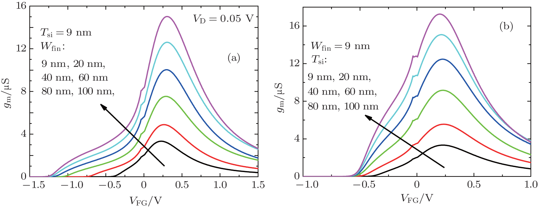
Fig. 4. Effects of (a) fin width and (b) film thickness on thin JL SOI FinFET. ND = 1019 cm−3, VD = 0.05 V, and VBG = 0 V.
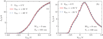
2.2.3. Effect of back gate

Figure 5(a) shows the comparison among the drain currents of a wide JL SOI FinFET versus front gate voltage for different back gate biases. For a positive back gate, the drain current shifts negatively and is higher due to the formation of an accumulation channel on the Si/BOX interface. For VBG < 0 V, the back channel is simply depleted (strong inversion would be obtained for VBG < −80 V according to Ref. [20]), and therefore the drain current decreases. For narrow JL SOI FinFET, the effect of back gate on the drain current weakens due to the domination of lateral gates as shown in Fig. 5(b).

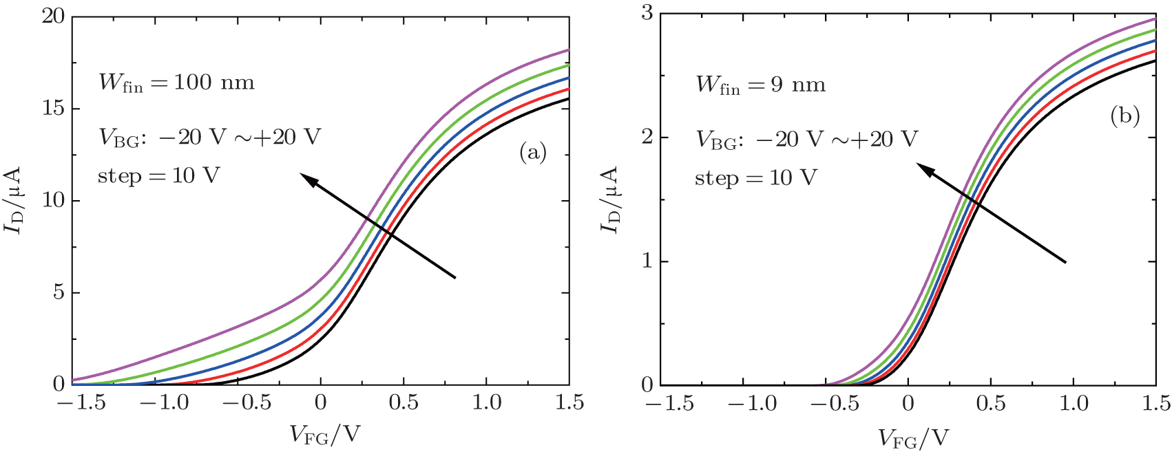
Fig. 5. Effects of back gate on the drain currents for (a) wide and (b) narrow JL SOI FinFETs. ND = 1019 cm−3, Tsi = 9 nm, and VD = 0.05 V.

This suppression of coupling effect between top and back gates is also visible in the comparison among gm(VFG) curves under different back gate biases (Fig. 6). For wide JL SOI FinFET, gm strongly varies with VBG only in the partial depletion mode (VFG < −0.3 V), but almost keeps unchanged in the accumulation mode (VFG > 0 V); for narrow JL FinFET, the variation of gm with VBG reduces. This is similar to the effect of fin width on the coupling effect between top and back gates reported in inversion-mode SOI FinFETs.[9] For a narrow and tall JL SOI FinFET, the lateral gates completely control the channel and therefore the coupling between top and back gate has a smaller effect as shown in Fig. 7.

Fig. 6. Effects of back gate on the transconductance for (a) wide and (b) narrow JL SOI FinFETs. ND = 1019 cm−3, Tsi = 9 nm, and VD = 0.05 V.
Fig. 7. Effects of back gate on narrow and tall JL SOI FinFET for (a) ID(VFG) and (b) gm(VFG). The coupling effect in narrow and tall JLSOI FimFEL has a small effect. ND = 1019 cm−3, VD = 0.05 V, and VBG = 0 V.

In summary, the coupling effect in JL SOI FinFET plays the same role as in the inversion-mode vertical DG SOI FinFET[9]

3. Modeling of 2D potential distribution in full depletion mode
3.1. Description of 2D potential model

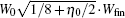
In the 2D analytical model of triple-gate SOI FinFETs proposed by Akarvardar et al.,[22] a parabolic potential variation between the two lateral gates is assumed. Here, we still assume that the potential profile between the two lateral gates is parabolic in the JL SOI FinFETs:

where φ(x,y) is the 2D body potential in heavily doped body.

The coefficients of Eq. (1) are determined by using the boundary conditions at the lateral gates:

Here, VFBF is the flat band voltage for the front gate, ɛsi is the silicon permittivity, Cox is the capacitance per unit area for the oxide of the front gate, and Wfin is the width of the fin. The two lateral gates are identical, so are the surface potentials: φ(−Wfin/2,y) = φ(Wfin/2,y) = φsf. Assume that corner effects, quantum-mechanical effects, substrate depletion (under the BOX) and drain bias effect can be ignored.[10,11,21] Using Eqs. (1)–(4), we obtain the coefficients in Eq. (1) as

In order to simplify the calculation, we define

η0 is actually equal to the ratio between Cfin and Cox. Cfin = ɛsi/Wfin is the “lateral” channel capacitance per unit area, defined in the 2D model of triple-gate SOI FinFETs.[22] Therefore, equation (1) can be rewritten as

Unlike the inversion-mode SOI FinFETs, the channel for JL SOI FinFET is heavily doped (∼ 1019 cm−3). Therefore, the fixed charge cannot be neglected in the full depletion region. Thus, the 2D Poisson equation for an n-channel junctionless FinFET is given by

Substituting Eq. (5) into Eq. (6) and letting x = 0, equation (6) is rewritten as

Considering boundary conditions between silicon and silicon dioxide (gate oxide and BOX), the solution of Eq. (7) has the form of

Here, C3 and C4 are the coefficients determined by the boundary conditions of the top (y = −Tsi/2) and bottom (y = Tsi/2) interfaces. Note that the thickness of the top gate oxide is equal to that of the lateral gate oxide in the modeled triple gate JL transistor.

in which VFBB is the flat-band voltage for back channel, CBOX and Ctox are respectively the capacitance per unit area for BOX and the oxide of the top gate.

Substituting Eq. (8) into Eqs. (9) and (10), we calculate C3 and C4 as

where

W0 represents the equivalent fin width when the channel is controlled by top and back gates (η0 = ɛsi/CoxWfin = Cfin/Cox and ). Therefore, equation (8) can be rewritten as

Substituting Eq. (14) into Eq. (5), the 2D potential distribution for an n-channel JL SOI FinFET is obtained analytically. Since we assume that there is no mobile charge in the full depletion mode, the potential model for p-type JL SOI FinFET is easily obtained by substituting the corresponding parameters of p-type transistors into Eq. (14).

3.2. Validation by simulations

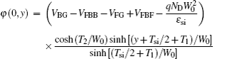
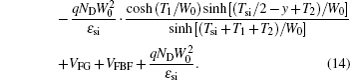
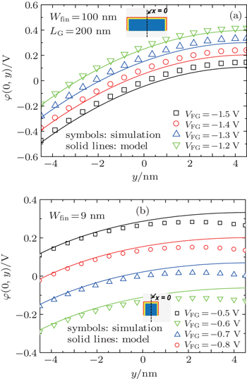
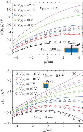
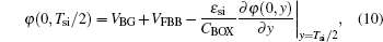
In order to validate our model for the potential distribution in JL SOI FinFET, we make a comparison of φ(0,y), the potential of the full depletion region along x = 0 (vertically cut in the middle of the channel, see Fig. 1), between model and simulations as shown in Fig. 8. For both wide (Fig. 8(a)) and narrow (Fig. 8(b)) JL SOI FinFETs, the modeled potentials follow the variation of simulated potential with front gate voltage.

Fig. 8. Potential profiles in the full depletion region along x = 0 (see Fig. 1(b)) each as a function of front gate voltage for (a) wide JL SOI FinFET (Wfin = 100 nm) and (b) a narrow JL SOI FinFET (Wfin = 9 nm). ND = 1019 cm−3, Tsi = 9 nm, VD = 0.05 V, and VBG = 0 V. y = −Tsi/2 is at the top of the film and y = Tsi/2 is at the BOX interface.

However, in the partial depletion region, the modeled potentials deviate from the simulated ones as shown in Fig. 9. This confirms that our model is valid and useful in the full depletion regime where the hypothesis in Eq. (6) is correct.

Fig. 9. Potential profiles in partially-depleted region along x = 0 (see Fig. 1) for variable front gate voltage. (a) Wfin = 100 nm and (b) Wfin = 9 nm. ND = 1019 cm−3, Tsi = 9 nm, VD = 0.05 V, and VBG = 0 V.

The effects of back gate on the potential in both wide and narrow JL SOI FinFETs are shown in Fig. 10. For each of the wide devices, an accumulation layer is formed when the back gate is positively biased (squares, circles and triangles in Fig. 10(a)), leading to the failure of full depletion approximation. More negative front gate bias (VFG < −1 V) is needed to obtain full depletion. When the channel at the bottom is depleted (VBG = − 10 & −20 V), the modeled potentials (circles and squares in Fig. 10(a)) show excellent agreement with the simulated ones. Compared with in the wide device, the effect of back gate on the body potential in narrow JL SOI FinFET is minor since the channel is mainly controlled by the lateral gates. However, the accumulation layer triggered by the positive back gate bias still leads to a small deviation at the bottom of the channel (y = 4.5 nm) as shown in Fig. 10(b).

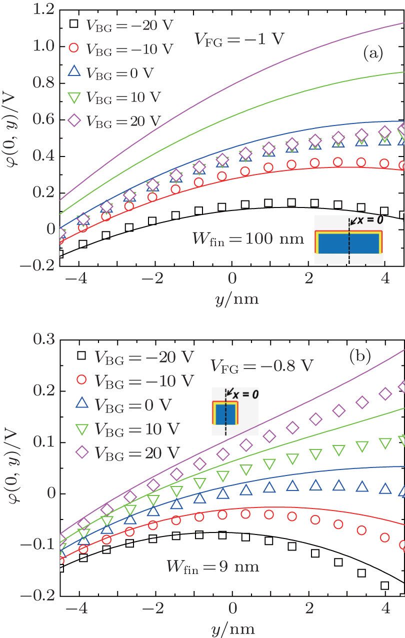
Fig. 10. Potential profiles in the full depletion region along x = 0 (see Fig. 1) each as a function of back gate voltage for devices with (a) Wfin = 100 nm and (b) Wfin = 9 nm. ND = 1019 cm−3, and Tsi = 9 nm.

In summary, this 2D potential model works in the full depletion regime with zero back gate bias or with VBG < 0 V (depletion at back interface).

4. Applications of 2D potential model

Since our 2D potential model successfully applies to the full depletion region of nano-channel JL SOI FinFET, we can use it to extract the threshold voltage, which is a key identifier to distinguish the full and partial depletion regions. Before using the model, we will introduce the current-voltage method proposed by Jeon et al.[23] to extract threshold voltage.

4.1. Conventional method to extract threshold voltage

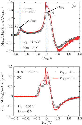
In a planar junctionless transistor, the threshold voltage is determined from the derivative of the transconductance (dgm/dVFG), shown in Fig. 11.[23] The first peak P1 corresponds to flat-band voltage, where the channel of the junctionless transistor just changes from surface accumulation to neutral state; the second peak P2 exhibits the threshold voltage, separating the partial region from the full depletion region (dotted line in Fig. 11(a)). This method works in the wide junctionless SOI FinFET (square in Fig. 11(a)), but fails in the narrow JL SOI FinFET where the coupling effect from lateral gates is extremely strong. As shown in Fig. 11(b) for a narrower fin, the two peaks tend to merge together, leading to difficulty in determining the threshold voltage and flat-band voltage. On the other hand, the experiments have demonstrated that high access resistance would lead to the disappearance of P2,[23] also making the threshold voltage extraction impossible.

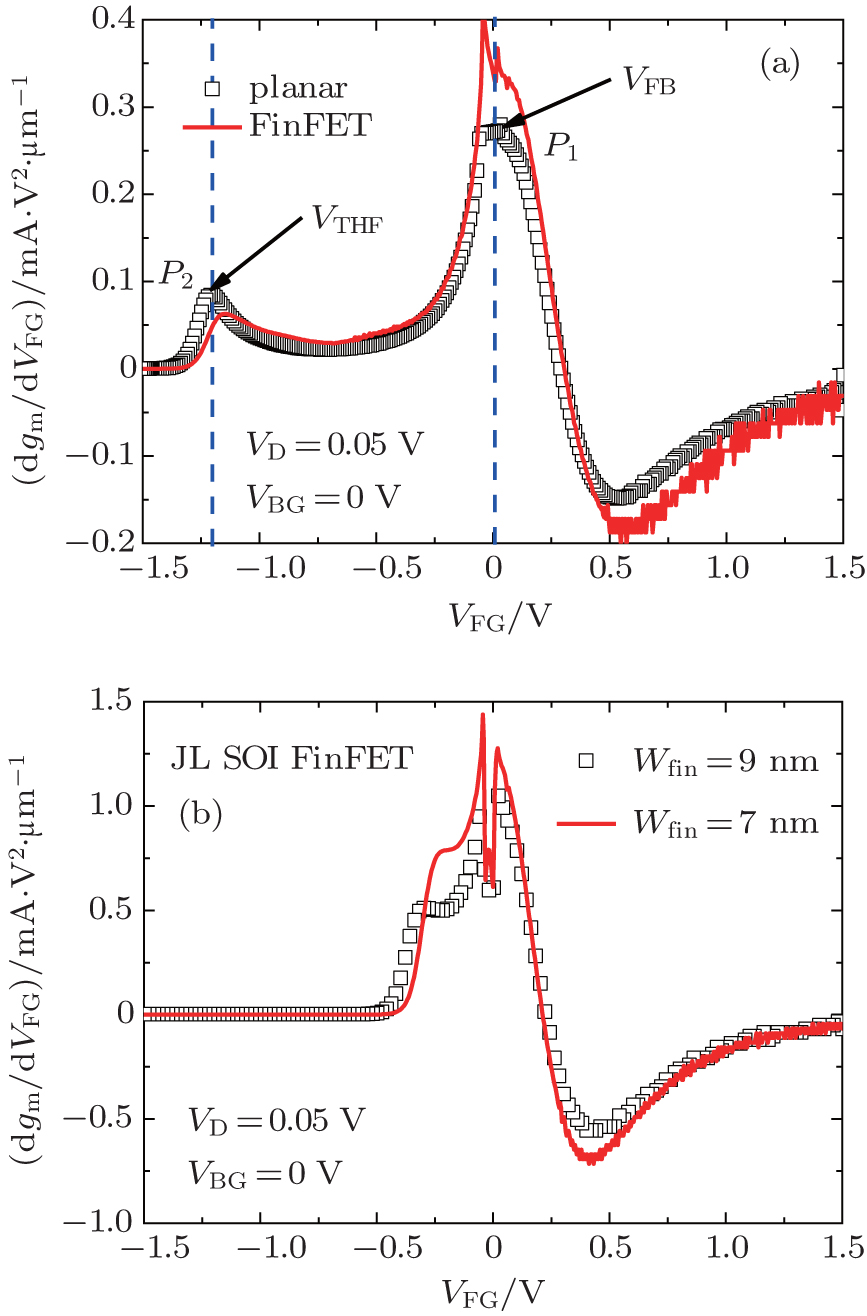
Fig. 11. (a) Plots of simulated dgm/dVFG versus VFG for a planar Si JL transistor and a wide JL SOI FinFET (Wfin = 100 nm); (b) plots of simulated dgm/dVFG versus VFG for two nano-channel junctionless SOI FinFETs (Wfin = 9 nm and 7 nm). Tsi = 9 nm, LG = 200 nm, and ND = 1019 cm−3.
4.2. Extraction of threshold voltage from the 2D potential model

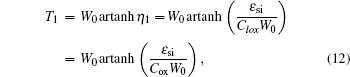
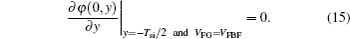
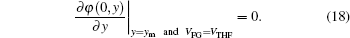
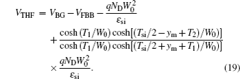
According to Ref. [15], the threshold voltage VTHF for a junctionless transistor can be defined as the front gate voltage when the channel is just fully depleted. It is given as the maximum potential at (x, y) = (0, −Tsi/2) for VBG = 0 V from Eq. (14), which corresponds to the point depleted finally. Therefore, we have

Substituting Eq. (14) into Eq. (15), the threshold voltage of the front gate can be modeled as

With the fin width shrinking, the control of lateral gates on the channel is enhanced, so the threshold voltage of the front channel shifts closer to the flat-band voltage (VFBF = 0 V) as shown in Fig. 12(a). The threshold voltage calculated from Eq. (16) coincides with the one extracted from the dgm/dVFG (Fig. 12(b)).[23] The deviation for wide fin (Wfin > 30 nm) can possibly be attributed to the effect of mobile charge. With a wider fin, the mobile charge density is larger for VFG = VTHF, leading to the imperfection of full depletion approximation (see the large subthreshold current for wide JL in Fig. 2(a)).

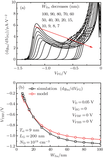
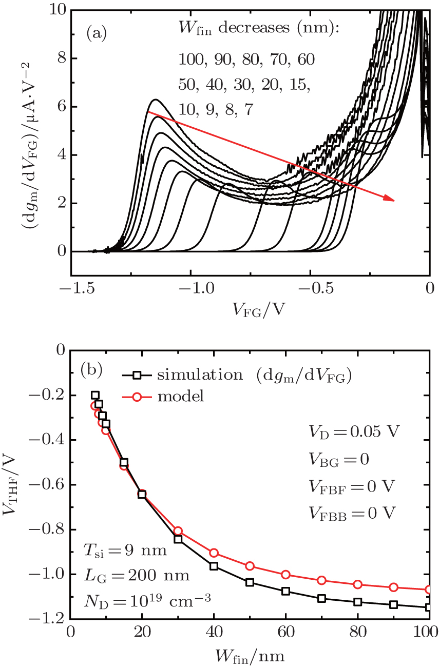
Fig. 12. (a) Plots of simulated dgm/dVFG versus VFG for different values of fin width Wfin, and (b) plots of threshold voltage of front gate extracted from Eq. (14) and the second peak of dgm/dVFG, versus. fin width.

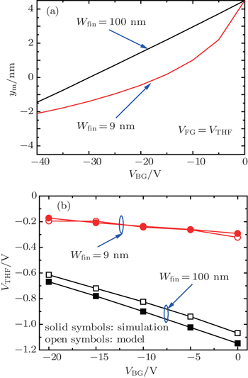
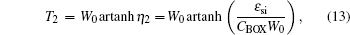
For depletion in the back channel, the point ym depleted finally lies in the middle of the channel along x = 0. Assume that the potential at ym does not vary with VFG nor VBG and is always equal to the Fermi potential φF, we have

For VFG = VTHF, the electric field at ym approximates to zero:

Combining Eqs. (17) and (18), we can obtain the relationship between ym and VBG as shown in Fig. 13(a). For larger VBG, ym shifts from the bottom of the fin toward the top. For a narrower fin, stronger depletion is induced by lateral gates and therefore this shift is larger. The threshold voltage is modeled as

Figure 13(b) shows the comparisons between the extracted threshold voltages obtained from the dgm/dVFG method and Eq. (19) under different values VBG. Our model shows good agreement in particular for nanowires. For a wide fin, the threshold voltage increases more negatively, which can be explained by the fact that the back gate helps to deplete the channel. For a narrower fin, the channel is mainly controlled by lateral gates and therefore the variation of threshold voltage is smaller.

Fig. 13. Plots of (a) ym versus VBG, and (b) comparisons of extracted VTHF between the dgm/dVFG method and our model (Eq. (19)).

It follows that equation (19) can be safely used to calculate the threshold voltage for VBG = 0 V or depletion at the back interface, if the flat-band voltages for front and back gates and the doping concentrations are known from technology.

4.3. Extraction of channel concentration from 2D potential model

Once the threshold voltage and flat-band voltage are known, the doping concentration of the channel can be determined. We can rewrite Eq. (16) as

In Table 1 summarized are the extracted doping levels for different fin widths, showing excellent agreement with the input doping concentration (1019 cm−3) for Wfin > 10 nm. For narrower JL FinFETs (Wfin < 10 nm), the extracted doping levels are a little underestimated. This can possibly be explained by the enhanced corner effects.

Table 1.

Extracted doping level from Eq. (20) for different fin widths.

.
5. Conclusions

In this paper, we prove the coupling effects for JL SOI FinFETs and propose a simple analytical model to determine the 2D potential profile within the body. The very good agreement obtained between simulated and modeling results validates the model. It works well in the full depletion region. The proposed models can be used for analysis of the coupling effect, characterization and optimization of geometry in any other heavily doped FinFETs. On the other hand, understanding these coupling effects and modeling them accurately are of great importance for applications. For example, increasing threshold voltage can reduce leakage current and power consumption. Conversely, lower operating bias is achieved with reduced threshold voltage. Also, we can co-integrate different functions into the same chip by tuning the threshold voltage.

Reference
1Colinge J PLee C WAfzalian AAkhavan N DYan RFerain IRazavi PO’Neill BBlake AWhite MAnne-Marie KBrendan MRichard M 2010 Nature Nanotechnology 5 225
2Doria R TPavanello M ATrevisoli R Dde Souza MLee C WFerain IAkhavan N DRan YRazavi PRan YKranti AColinge J P 2011 IEEE Trans. Electron Dev. 58 2511
3Kranti ALee C WFerain IYan RAkhavan NRazavi PYu RArmstrong G AColinge J P 2010 Electron Lett. 46 1491
4Baek D JDuarte J PMoon D IKim C HAhn J HChoi Y K 2012 Appl. Phys. Lett. 100 213703
5Lim H KFossum J G 1983 IEEE Trans. Electron Dev. 30 1244
6Fernandez CRodriguez NOhata AGamiz FAndrieu FFenouillet-Beranger CFaynot OCristoloveanu S 2013 IEEE Electron Dev. Lett. 34 840
7Parihar M SLiu F YNavarro CBarraud SBawedin MIonica IKranti ACristoloveanu S2015Proceedings of 45th Europe Solid-State Device ConferenceWien, Austria61
8Park S JJeon D YMont‘es LBarraud SKim G TGhibaudo G 2013 Solid-State Electron. 87 74
9Chang S JBawedin MGuo Y FLiu F YAkarvardar KLee J HIonica ICristoloveanu S 2014 Solid-State Electron. 97 88
10Lee C WAfzalian AAkhavan N DYan RFerain IColinge J P 2009 Appl. Phys. Lett. 94 053511
11Lee C WFerain IAfzalian AYan RAkhavan N DRazavi PColinge J P 2010 Solid-State Electron. 54 97
12Sallese J MChevillon NLallement CIñíguez BPregaldiny F 2011 IEEE Trans. Electron Dev. 58 2628
13Colinge J P 1990 IEEE Trans. Electron Dev. 37 718
14Duarte J PChoi S JChoi Y K 2011 IEEE Trans. Electron Dev. 58 4219
15Holtij TSchwarz MKloes AIñíguez B 2013 Solid-State Electron. 90 107
16Trevisoli R DDoria R Tde Souza MDas SFerain IPavanello M A 2012 IEEE Trans. Electron Dev. 59 3510
17Colinge J PKranti AYan RLee C WFerain IYu RAkhavan N DRazavi P 2011 Solid-State Electron. 65 33
18Jeon D YPark S JMouis MBarraud SKim G TGhibaudo G 2013 Solid-State Electron. 81 58
19Synopsys Inc.TCAD Sentaurus User Manual G-2012.06 2012
20Liu F YDiab AIonica IAkarvardar KHobbs COuisse TMescot XCristoloveanu S 2013 Solid-State Electron. 90 65
21Akarvardar KMercha ACristoloveanu SGentil PSimoen ESubramanian VClaeys C 2007 IEEE Trans. Electron Dev. 54 767
22Hu W DChen X SZhou X CQuan Z JWei L 2006 Microelectron. 37 613
23Jeon D YPark S JMouis MBerthomé MBarraud SKim G TGhibaudo G 2013 Solid-State Electron. 90 86