
Inverted polymer solar cells with employing of electrochemical-anodizing synthesized TiO2 nanotubes
[Ahmadi Mehdi†,  , Rashidi Dafeh Sajjad, Fatehy Hamed]
, Rashidi Dafeh Sajjad, Fatehy Hamed]
|
|


† Corresponding author. E-mail:
An inverted structure of polymer solar cells based on Poly(3-hexylthiophene)(P3HT):[6-6] Phenyl-(6) butyric acid methyl ester (PCBM) with using thin films of TiO2 nanotubes and nanoparticles as an efficient cathode buffer layer is developed. A total of three cells employing TiO2 thin films with different thickness values are fabricated. Two cells use layers of TiO2 nanotubes prepared via self-organized electrochemical-anodizing leading to thickness values of 203 and 423.7 nm, while the other cell uses only a simple sol–gel synthesized TiO2 thin film of nanoparticles with a thickness of 100 nm as electron transport layer. Experimental results demonstrate that TiO2 nanotubes with these thickness values are inefficient as the power conversion efficiency of the cell using 100-nm TiO2 thin film is 1.55%, which is more than the best power conversion efficiency of other cells. This can be a result of the weakness of the electrochemical anodizing method to grow nanotubes with lower thickness values. In fact as the TiO2 nanotubes grow in length the series resistance (Rs) between the active polymer layer and electron transport layer increases, meanwhile the fill factor of cells falls dramatically which finally downgrades the power conversion efficiency of the cells as the fill factor falls.
In recent years polymer solar cells (PSCs) have gained a great deal of attention due to their special properties such as light weight, low cost, elasticity, low environmental load and large scale production potential.[1–3] On the other hand there are still challenges to PSCs for making them achieve long term stabilities and high power conversion efficiencies (PCEs).[4] The main problems of PSCs lie in the material instability used in different layers like the PEDOT: PSS layer and technical difficulties in implementing normal cell architecture. PEDOT: PSS has hygroscopic properties making ITO/PEDOT: PSS sensitive to ambient conditions, meanwhile the acidic nature of PEDOT: PSS increases the degradation rate of the ITO/PEDOT: PSS. Also PEDOT: PSS degrades under UV illumination and has inhomogeneous electrical properties.[5–8] The other problem that must be solved in normal architecture of PSCs is the oxidation of low work function top metal oxides in the air.[9]
Adopting an inverted architecture and inserting a buffer layer between active layers and electrodes is a technique for solving these problems.[3,9] N-type metal oxides and alkali metal compounds can be used as an electron selective and hole-blocking layer. Layers of ZnO,[3,5,9–11] TiO2,[12–14] Cs2CO3,[15] LiF,[8] and In2S3[16] are widely used in PSCs. Within these materials TiO2 shows that it is a promising electron-selective and hole-blocking material as in addition to optical transparency and high electron mobility, it has chemical and physical stability. TiO2non-toxicity and its inexpensive largescale production are additional advantages over some other materials. Also TiO2 has substantial oxygen and water protection because of photo-catalysis combination and inherent oxygen deficiency.[17–20]
These unique qualities encouraged us to use TiO2 nanotubes in fabricating solar cells as the electron transport layer (ETL). As the active layer is deposited in the inner and outer surface of the nanotubes, this will lead to a higher inter-facial area which may increase the charge carriers and finally increases the PCE of the cell. Different methods were adopted to fabricate cells with TiO2 thin films and nanotubes such as atomic layer deposition,[13,19] magnetron sputtering,[12,21] doctor-blade method,[22] and spin coating.[23]
As is well known anodizing in fluorides can be realized in self-organizing conditions, so it can be employed to grow highly ordered arrays of closely packed vertically aligned tubes. Therefore we are to use self-organized electrochemical anodizing for growing the TiO2 nanotubes (TNTs) with different lengths which are the cathode buffer layer in our cells. Meanwhile we prepare another cell with TiO2 thin film to discuss the experimental results, especially the PCE of the cells.
In this work, the sol–gel method is used for fabricating the TiO2 nanoparticles (NPs) and TiO2 thin film Nps. For this purpose, 5-ml of titanium tetraisopoxide (TTIP, with 99.7% purity purchased from sigma Aldrich) were mixed in 80 ml of n-heptane as a solvent and stirred for 60 min. Then 1-ml of deionized water was added drop by drop. The molar ratio of TTIP: H2O was maintained at 1:5. Prior to the deposition of TiO2 NPs, ITO/glass substrates were ultrasonically cleaned in acetone and isopropanol for 15 min. Afterwards, thin films of TiO2 NPs were deposited on an ITO/glass substrate via the doctor blade method. Then thin films of NPs were aged at 35 °C for 24 h and then dried at 100 °C for 8 h and annealed at 450 °C in the ambient condition in the presence of air for 60 min to remove any impurities from TiO2 paste. The thickness of the TiO2 thin film NPs was 100 nm.
Afterward TiO2 NTs electrode was prepared by twostep anodization. A titanium foil with a thickness of 0.25 mm and 99.7% purity was purchased from Sigma Aldrich. The foil was cleaned by sonication in a solution of ethanol, methanol, acetone and isopropanol for 30 min. Anodization was performed using clean Ti foil as the anode and a Pt sheet with the same size as cathode in an electrolyte of 0.27-M NH4F and water/ethyl glycol (50:50). A voltage of 20 V was applied for 60 min. Anodization equipment was composed of a Keithley programmable voltage source and a working electrode modified by a Platinum foil as the counter electrode with a fixed distance of 1.5 cm.
Next, for transfering TiO2 NTs electrodes onto the ITO/glass substrate, TiO2 NTs were detached from the bottom Ti foil via secondary anodization at 20 V in an electrolyte consisting of 0.27-M NH4F and water/ethyl glycol (50:50). The detached TiO2 NTs were cleaned with ethanol and deionized water and then transferred to an adhesion layer on the ITO/glass substrate. To increase the adhesion between the TiO2NTs and the ITO/glass substrate, the TiO2 NTs electrode was annealed at 450 °C for 60 min after being transferred. Finally samples were cleaned several times by ethanol and deionized water and dried in a nitrogen stream.
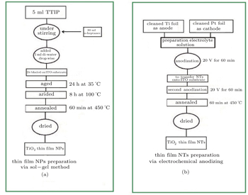
Finally, in order to prepare an active layer of the solar cells, P3HT and PCBM were dissolved in chlorobenzene separately. Then a 60-°C hot plate was used for stirring dissolved solutions overnight. At a weight ratio of 1:0.9, we blended the solutions. Afterward we used the 60-°C hot plate to stir the solutions again. The active layer was deposited on ETL in air via the doctor blade method at a speed of 15 mm/s and temperature of 60 °C. The overall thickness of the active layer was measured to be 120 nm. Then a thin layer of PEDOT:PSS as the hole-transport layer was deposited on the active layer with a speed of 15 mm/s and temperature of 60 °C. Inert atmosphere annealing on a hot plate at 140 °C was employed for 5 min. Thermal evaporation at ∼ 5 × 10⁻⁶ mbar (1 bar = 105 Pa) and a shadow mask were used to deposit an Ag electrode, which resulted in an active area of 10.4 mm2. The synthesis procedures of TiO2 NPs and NTs thin films are summarized in Fig.
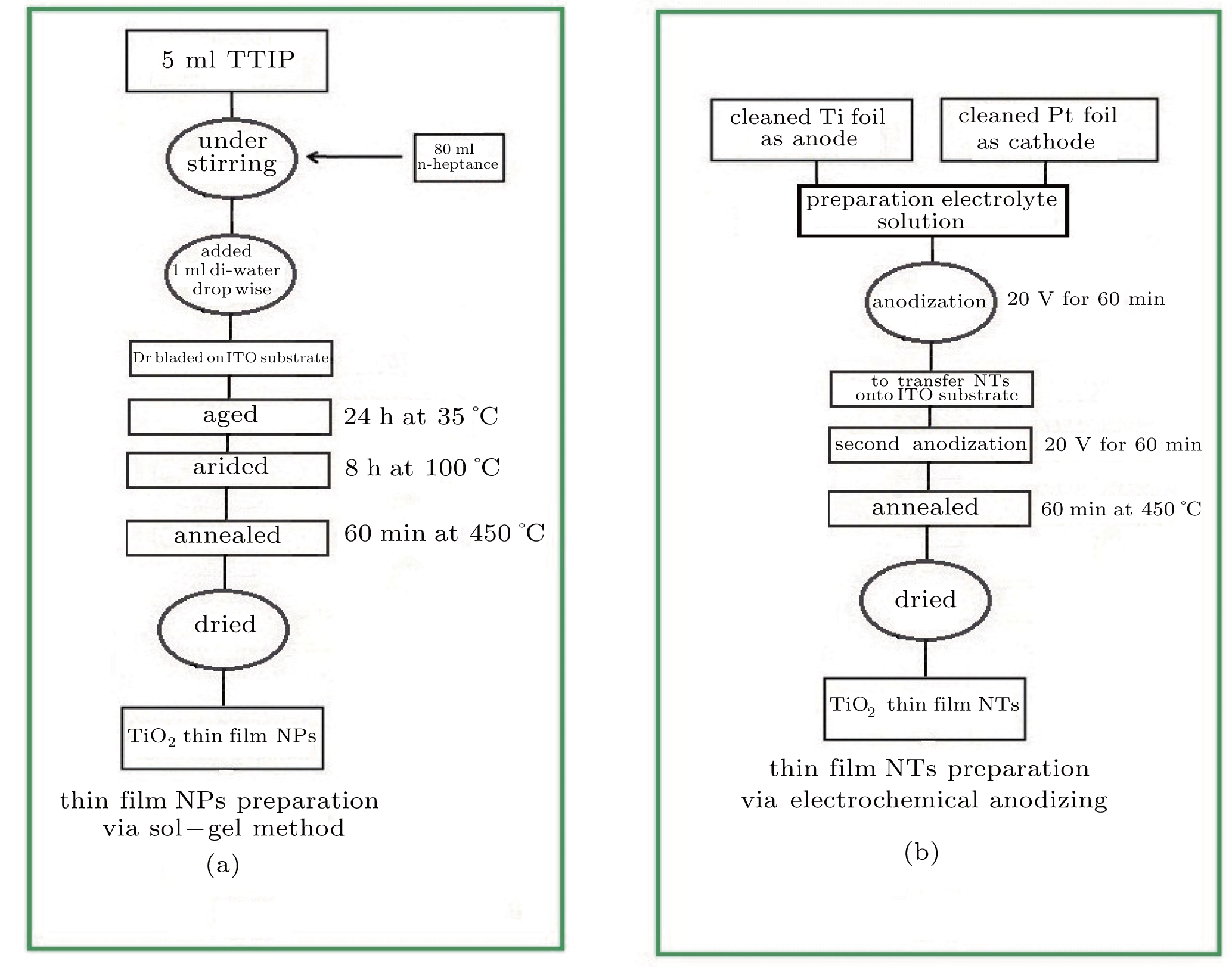 | Fig. 1. Synthesis procedures of TiO2 NPs thin film and TiO2 NTs. |
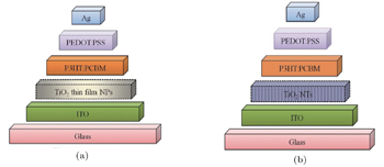
Also, the structure of the inverted polymer solar cells employing TiO2 thin film and TiO2NTs are shown in Fig.
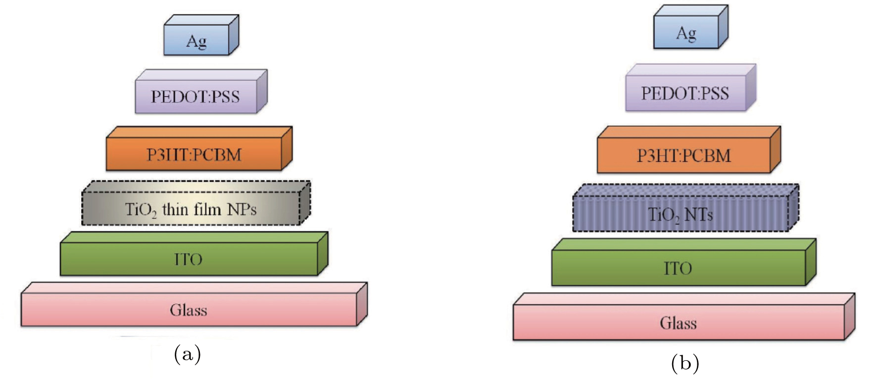 | Fig. 2. Structures of the inverted polymer solar cells employing a) TiO2 NPs thin film and b) TiO2NTs. |
The structures of TiO2 NPs thin film and TiO2 NTs are analyzed using x-ray diffraction (XRD) Model Philips MPD PW 3040 in a 2θ range from 20° to 80° at a scan rate of 0.02°/s. The surface morphologies of the TiO2 NTs and NPs thin film are observed by using a scanning electron microscope (SEM) model ultra plus-Zeiss SMT. The UV-VIS radiation was recorded using a Perkin Elmer-Lambda 950 spectrometer in a 200-nm–800-nm wavelength range. Current density–voltage (J–V) characteristics were measured with a measurement source unit from Botest. Finally, an Oriel Sol 1A solar simulator was used for providing AG1.5 spectra at 100 mW/cm2 for cell illumination.
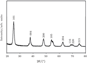
The crystalline structure of TiO2 thin film is revealed by XRD measurement. Figure
 | Fig. 3. The XRD pattern of the synthesized TiO2 thin film. |
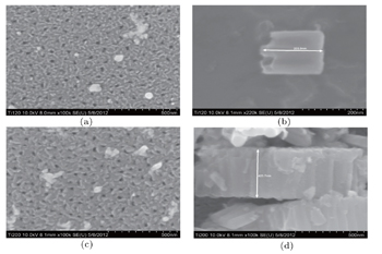
Figure
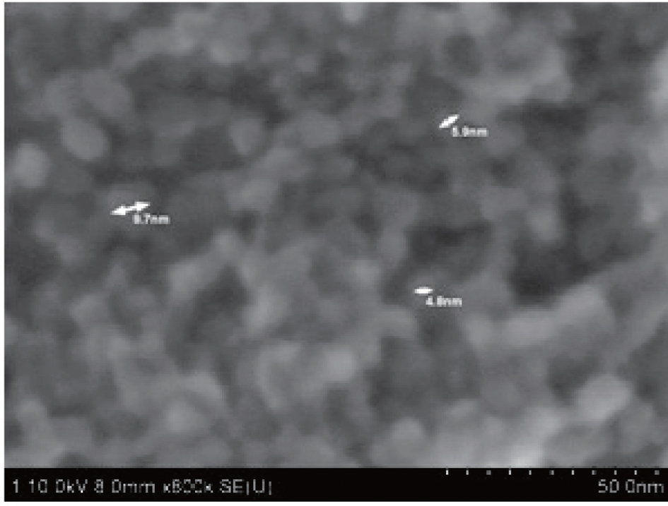 | Fig. 4. The SEM image of TiO2 NPs thin film with a thickness of 100 nm. |
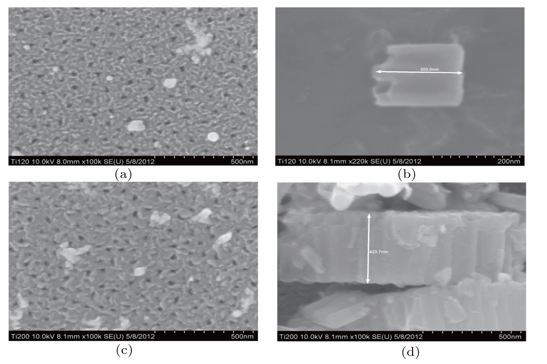 | Fig. 5. Top and cross section view SEM images of TiO2 NTs with thickness values of 200 nm and 400 nm. |
Top and cross section view SEM images of TiO2 NTs with thickness values of 200 nm and 400 nm.
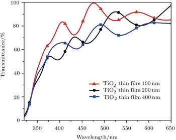
Optical properties of TiO2 NPs thin film with a thickness of 100 nm and TiO2 NTs with thickness values of 200 nm and 400 nm on ITO/glass substrate are studied by measuring the UV-VIS spectra as shown in Fig.
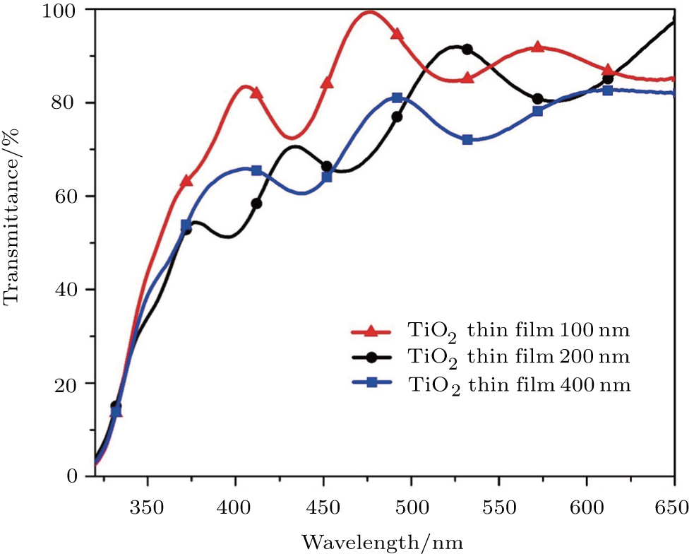 | Fig. 6. UV-VIS spectra of TiO2 NPs thin film and TiO2 NTs in diverse thickness values. |
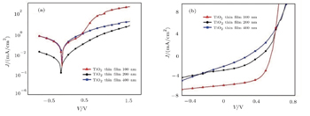
The variations of current-density with voltage of our cells are shown in Fig.
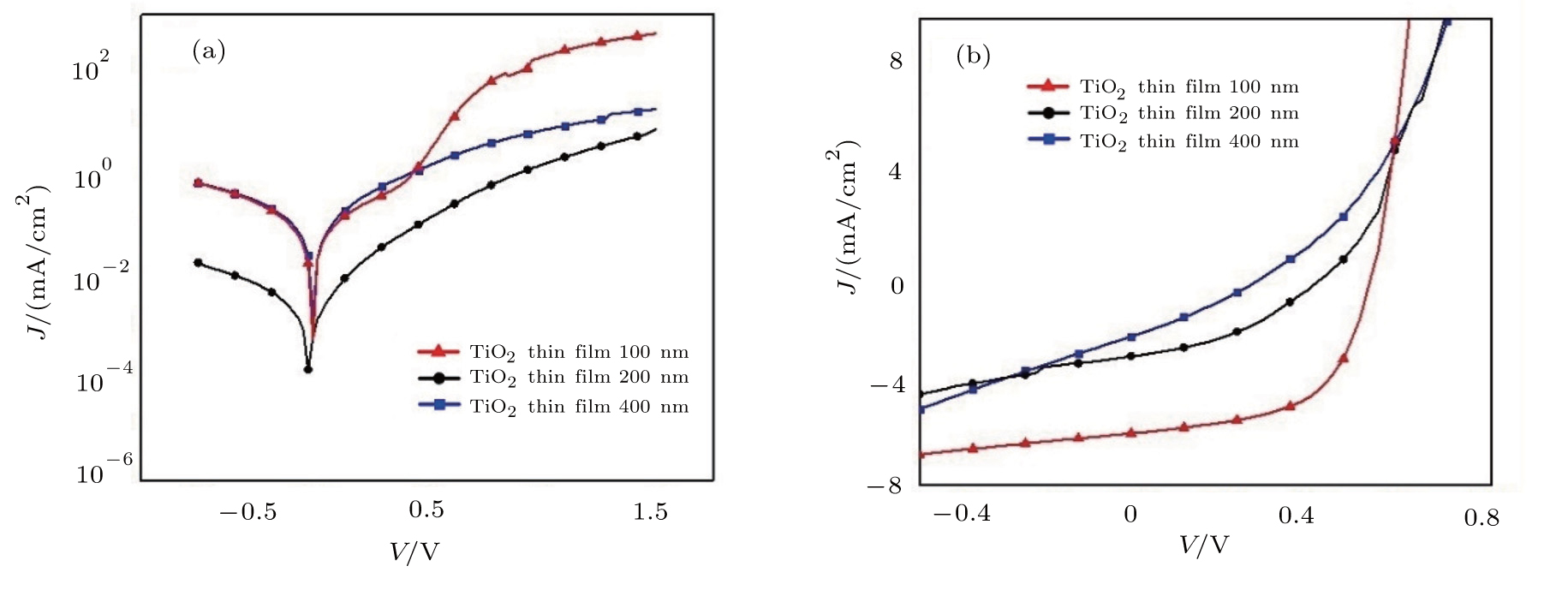 | Fig. 7. The J–V curves of inverted solar cells using different ETLs in the cases (a) without illumination, (b) under simulated solar irradiation of AM1.5G. |
| Table 1. Briefed key parameters of the devices with different TiO2 ETLs. . |
Well-aligned TiO2 NTs are synthesized successfully on the ITO coated glass substrate via self-organized electrochemical anodizing and doctor blading method. Also the sol–gel method is used for fabricating the TiO2 NPs thin film. Different TiO2 substrate thickness values led to different lengths of TiO2 nanotubes. The characterization results of XRD, SEM and UV-VIS transmittance spectroscopy verify the successful growth of TiO2 nanotubes and NPs thin film. The XRD pattern discloses that TiO2 thin film has the structure of anatase. Also the average size (diameter) of TiO2 NPs thin film is estimated to be about 10 nm from the SEM image. The length of TiO2 NTs is calculated from the SEM cross sectional images to be about 203 nm and 423.7 nm for diverse thickness values of NTs. According to the UV-VIS spectrum, TiO2 NPs thin film shows better transmittance than TiO2 NTs. The superior transmittance of TiO2 NPs thin film can be one of the reasons that the cell using this ETL shows better PCE. Unlike the proper growth of the nanotubes, PCE of the cells are not so sufficient as expected. The main reason for this failure is the increase of the series resistance of TiO2 NTs as their lengths are not appropriate. Also, the results indicate that the device using TiO2 NPs thin film has a higher PCE than other devices and also we observe that the PCE of the device is reduced by increasing the thickness of the thin film.
| 1 | |
| 2 | |
| 3 | |
| 4 | |
| 5 | |
| 6 | |
| 7 | |
| 8 | |
| 9 | |
| 10 | |
| 11 | |
| 12 | |
| 13 | |
| 14 | |
| 15 | |
| 16 | |
| 17 | |
| 18 | |
| 19 | |
| 20 | |
| 21 | |
| 22 | |
| 23 |