

Optoelectronic properties of SnO2 thin films sprayed at different deposition times
[Abdelkrim Allag, Rahmane Saâd†,  , Abdelouahab Ouahab, Hafida Attouche, Nabila Kouidri]
, Abdelouahab Ouahab, Hafida Attouche, Nabila Kouidri]
|
|


† Corresponding author. E-mail:
This article presents the elaboration of tin oxide (SnO2) thin films on glass substrates by using a home-made spray pyrolysis system. Effects of film thickness on the structural, optical, and electrical film properties are investigated. The films are characterized by several techniques such as x-ray diffraction (XRD), atomic force microscopy (AFM), ultraviolet-visible (UV–Vis) transmission, and four-probe point measurements, and the results suggest that the prepared films are uniform and well adherent to the substrates. X-ray diffraction (XRD) patterns show that SnO2 film is of polycrystal with cassiterite tetragonal crystal structure and a preferential orientation along the (110) plane. The calculated grain sizes are in a range from 32.93 nm to 56.88 nm. Optical transmittance spectra of the films show that their high transparency average transmittances are greater than 65% in the visible region. The optical gaps of SnO2 thin films are found to be in a range of 3.64 eV–3.94 eV. Figures of merit for SnO2 thin films reveal that their maximum value is about 1.15 × 10⁻⁴ Ω−1 at λ = 550 nm. Moreover, the measured electrical resistivity at room temperature is on the order of 10−2 Ω·cm.
Transparent conducting oxides have been a research subject for years.[1–4] SnO2 is of interest because it is a naturally non-stoichiometric prototypical transparent conducting oxide. It has a wide band gap of 3.6 eV, plasma frequency in the IR region and when suitably doped, it can be used as both a P-type and N-type semiconductor.[5,6] SnO2 thin film is transparent in the region above 400 nm, which is the region of interest for electrochromic devices. Doping tin oxide with fluorine, chlorine, antimony etc.[7,8] as donor impurities yields films with a low sheet resistance.[9]
SnO2 films were used extensively as transparent electrodes in display devices like liquid crystal displays (LCDs) and as transparent active layers in SnO2 silicon solar cells,[10] thin film resistors, antireflection coatings, photochemical devices and electrically conductive glass.[11] Among the varieties of methods that have been proposed for depositing films of SnO2, spray pyrolysis has been found to be attractive in the sense of its simplicity and low cost.
The aim of this research is to establish a relationship between the film thickness and the film properties. In order to achieve this goal, tin oxide films are prepared by a spraying method at various deposition times ranging from 1 min to 5 min. The properties of the films are characterized by x-ray diffraction analysis (XRD), atomic force microscopy (AFM), ultraviolet-visible (UV–Vis) spectroscopy, and four-point conductivity measurement methods.
The tin oxide films were prepared using a home-made spray pyrolysis system. In this deposition technique, liquid precursors were sprayed by atomization processes and condensed by thermal decomposition on substrates maintained at elevated temperatures. The sprayed micro-droplets reaching the hot substrate surface underwent pyrolytic decomposition and formed a single crystallite or a cluster of crystallites of the sprayed materials. Stannous chloride (SnCl2, 2H2O) was used as a precursor for tin. This tin precursor dissolved in distilled water with adding a few drops of hydrochloric acid (HCl). The precursor concentration was fixed to be 0.15 mol/l. All spray solutions were magnetically stirred to obtain homogenous solutions. The resulting solutions were sprayed on glass substrates. The normalized distance of 30 cm between the spray nozzle and the substrates was maintained. The spray solution quantity of 100 ml was kept fixed during the growth. Filtered compressed air was used as the gas carrier. The deposition time was varied from 1 to 5 min. The substrate (working) temperature was maintained at 500 °C by an electronic temperature controller connected to the heater. After deposition, the coated substrates were cooled down naturally to room temperature.
The formation of SnO2 film from a SnCl2 solution gives rise to a transitory formation of the compound SnO. The relevant chemical reactions are[12–14]


The structural characterization of the SnO2 thin films was carried out by x-ray diffraction (XRD) measurements with using a BRUKER D8 ADVANCE diffractometer with Cu Kα radiation (λ = 1.541838 Å). The diffractometer reflections were measured at room temperature and the values of 2θ were varied between 20° and 80°. The surface morphologies of the films were observed using an A100 Atomic Force Microscope. The dc electrical resistivity was measured in the dark and at room temperature with a four-point probe technique. The film optical transmittance was recorded by using a SHIMADZU 1800 UV-visible scanning spectrophotometer in a spectral region between 200 nm and 800 nm.
Each of the films deposited on glass substrates are physically stable and have a good adherence to the substrate (hardly peeled with the scotch tape test).
The film thickness (t) of SnO2 thin film is measured by the gravimetric method using the relation

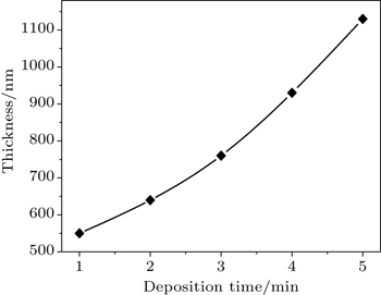
The thickness values of the films are found to be between 550 nm and 113 nm as listed in Table
| Table 1. Values of lattice parameters a and c, interplanar distance d, thickness and intensity of the films. . |
 | Fig. 1. Plot of film thickness versus deposition time for estimating growth velocity. |
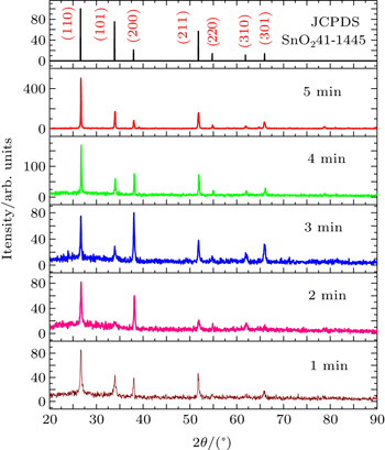
To investigate the crystalline quality of the films with various deposition times, XRD analysis is made. The resulting spectra are shown in Fig.
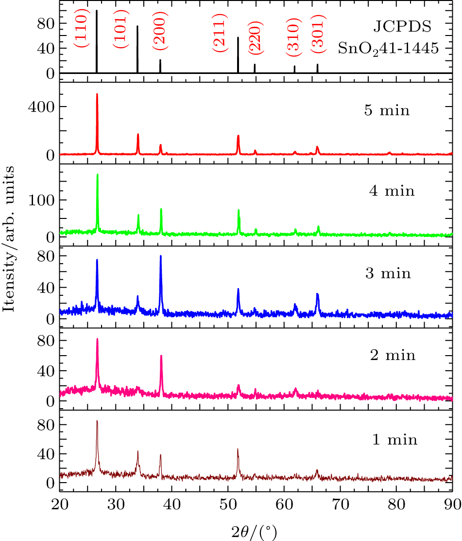 | Fig. 2. X-ray diffraction patterns of SnO2 thin films with different film thickness values. |
The (110) is the most intense peak which is observed for all samples, and other peaks assigned as (101), (200), (211), (220), (310), and (301) orientations are also observed with increasing film thickness. This can be attributed to the density of the atoms in the (110) plane, which is the highest in the atom densities in all planes of the rutile crystal structure; therefore, the surface energy of the (110) plane is the lowest.
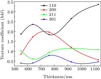
The reflection intensity for each peak contains information about the preferential or random growth of polycrystalline thin films, which is investigated by calculating the texture coefficient TC(hkl) for the plane from the following equation:[15]

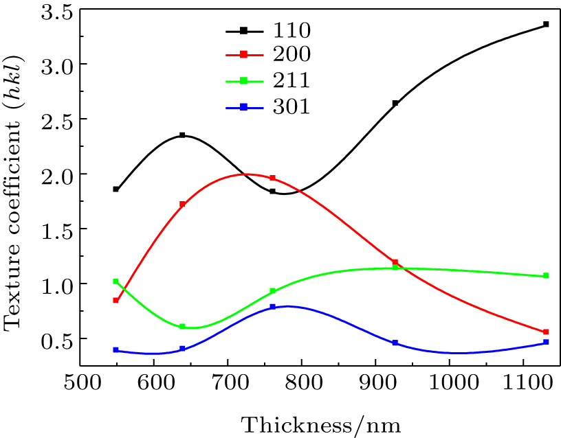 | Fig. 3. Variations of TC values with film thickness. |
The intensity of thin film can be estimated from the following equation:

The lattice constants a and c for tetragonal phase structure are determined from Eq. (

The grain sizes of the films are calculated from the highly textured (110) peaks from the Scherer formula:[19]

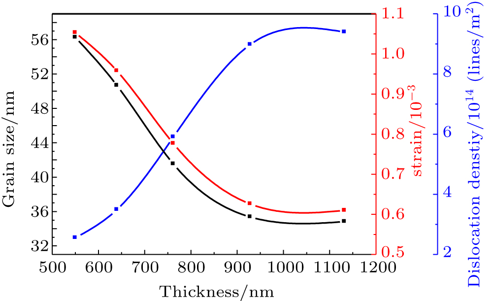 | Fig. 4. Variations of grain size, strain and dislocation density with film thickness. |
The misfit strain is one of the most important factors adversely affecting the structural properties, which results from the geometric mismatch at inter phase boundaries between crystalline lattices of films and substrate.[20] These stresses can cause strains in the films. The strain (ɛ) value of SnO2 film for the (110) peak is calculated from the following formula:[21]

The dislocation density (δ) is defined as the length of dislocation line per unit volume (lines/m2). For the (110) peak, the dislocation density (δ) of the film is estimated from the following equation:[22]

For the (110) peak, the greater value of δ is calculated to be as high as 9.22 × 10¹⁴ lines/m2 for 1-min time deposition, and the smallest value as low as 3.09 × 10¹⁴ lines/m2 for 5 min time deposition.
Figure
Figure
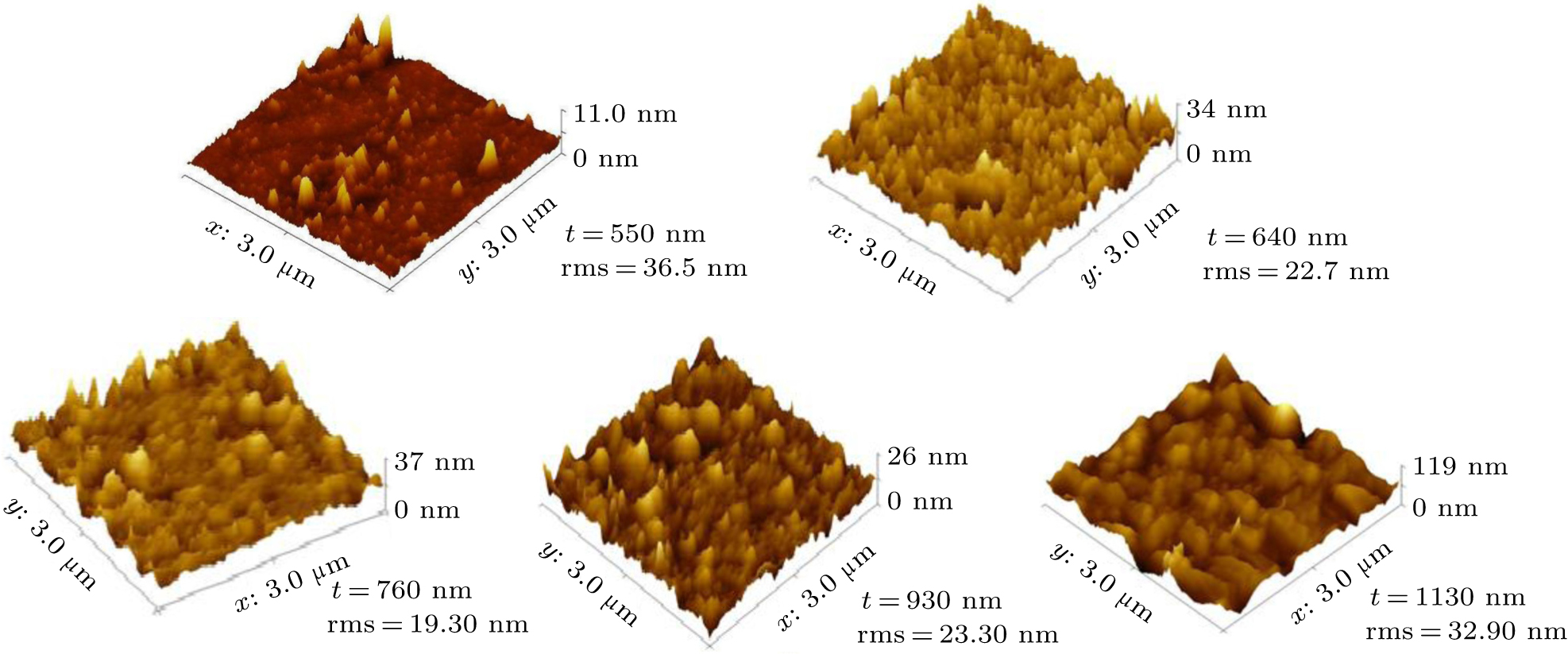 | Fig. 5. Atomic force microscope (AFM) surface images of SnO2 films with different thickness values. |
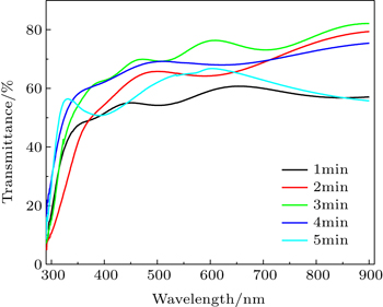
Optical properties of SnO2 thin films are investigated by UV–VIS spectrophotometer at room temperature.
Figure
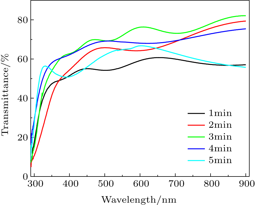 | Fig. 6. Optical transmittances versus wavelength for SnO2 films with different thickness values. |
In order to find the band gap (Eg) values of films, initially the absorption coefficient (α) should be identified by the relation:[23]


The film thickness effect on the absorption measurement is investigated. As seen from Table
| Table 2. Values of optical parameters of SnO2 thin films. . |
The localised states near the band edge cause the band tails to occur in material band diagram. These band tail states are responsible for the absorption in the low energy range. In this range the absorption coefficient is given as:[26]

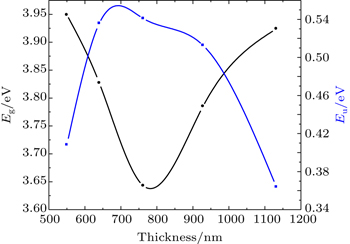
Figure
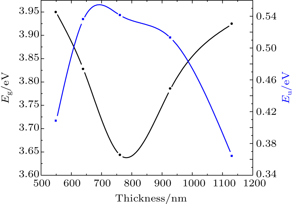 | Fig. 7. Variations of band gap and Urbach tail with film thickness. |
The refractive index (n) of semiconducting material is very important in the determining of their optical properties. Knowledge of (n) is essential in the design of heterostructure lasers, in optoelectronic devices, as well as in solar cell applications. The refractive index of the film can be calculated from the following Herve and Vandamme relation:[29,30]

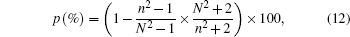
The porosity is the property of a material with small-size pores or cavities which can contain fluids (liquid or gas). The volume porosity p(%) of the film is estimated from the refractive index n by using the Lorentz–Lorentz relationship:[31]
From Table
The change in the porosity can be explained by the fact that in the first case the particles arriving at the substrate spread easily on the substrate; therefore, a denser layer is formed. When the deposition time is increased, the arriving droplets must spread on the surface of the film deposited already and discrete particles are formed, which increases the roughness and leads to a more porous morphology.
The electrical properties of SnO2 films are investigated by the four-point probe method and it is found that all samples have n-type conductions. The values of sheet resistance and resistivity of the films are given in Table
| Table 3. Values of electrical parameters of SnO2 thin films. . |
For measuring the sheet resistance (Rsh) by the linear four-point probe technique, the current (I) is applied between the outer two leads and the potential difference (V) across the inner two probes is measured. Since negligible contact and spreading resistance are associated with the voltage probes, one can obtain a fairly accurate estimation of Rsh from the following relation:

The resistivity values of SnO2 films are calculated from the following formula:

The tin oxide is widely used in solar cells as a front contact material. To determine the efficiency of SnO2 in usage as a front contact, the figure of merit parameter is built up by Haacke as follows:[36]

The figure-of-merit values of films with different thickness values in the present study are calculated by Eq. (
It is clear that the resistivity increases with increasing film thickness. The resistivity variation is attributed to carrier concentration and/or mobility changing. These parameters are closely related to the film structure. The SnO2 grains are relatively closely distributed on the surface and they grow along the densest plane of the rutile structure, which causes the carrier density to reach a lowest value and/or the electron traps to increase with film thickness increasing.
Polycrystalline thin films of SnO2 with different thickness values are prepared at 500 °C on glass substrates using a home-made spray pyrolysis apparatus. The influence of thickness on the film physical properties is investigated by using XRD, AFM, four-point and UV-vis spectrophotometer measurements. Film thickness values are estimated by the gravimetric method to be between 550 nm and 1130 nm. XRD characterization reveals that the SnO2 films are of polycrystals each with a cassiterite tetragonal crystal structure and preferential orientation along the (110) plane. From electrical measurements, it is found that the film has n-type electrical conductivity; a maximum figure-of-merit value (as high as 1.15 × 10⁻⁴ Ω−1) is obtained for SnO2 thin film with 760-nm thickness. All films have high transmissions greater than 65% in the visible region, indicating that they are good-quality films. The highest refractive index and optical band gap values are also found to be 2.175 eV and 3.64 eV, respectively, for the sample deposited at a deposition time of 3 min.
From these results, it is concluded that favorable structural, electrical and optical properties of SnO2 thin films make them a very suitable candidate for usage in optoelectronic devices and solar cell applications.
| 1 | |
| 2 | |
| 3 | |
| 4 | |
| 5 | |
| 6 | |
| 7 | |
| 8 | |
| 9 | |
| 10 | |
| 11 | |
| 12 | |
| 13 | |
| 14 | |
| 15 | |
| 16 | |
| 17 | |
| 18 | |
| 19 | |
| 20 | |
| 21 | |
| 22 | |
| 23 | |
| 24 | |
| 25 | |
| 26 | |
| 27 | |
| 28 | |
| 29 | |
| 30 | |
| 31 | |
| 32 | |
| 33 | |
| 34 | |
| 35 | |
| 36 |