S Honey, S Naseem, A Ishaq, M Maaza, M T Bhatti, D Wan. Large scale silver nanowires network fabricated by MeV hydrogen (H+) ion beam irradiation. Chinese Physics B, 2016, 25(4): 046105
Permissions
Large scale silver nanowires network fabricated by MeV hydrogen (H+) ion beam irradiation
S Honey1, 2, 3, 4, †, , S Naseem1, ‡, , A Ishaq2, 3, 4, M Maaza3, 4, M T Bhatti5, D Wan6
Center of Excellence in Solid State Physics, University of the Punjab, Lahore, Pakistan
National Center for Physics, Quaid-i-Azam University, Islamabad 44000, Pakistan
UNESCO–UNISA Africa Chair in Nanosciences/Nanotechnology, College of Graduate Studies, University of South Africa, Muckleneuk ridge, P. O. Box 392, Pretoria, South Africa
Nanosciences African Network (NANOAFNET), iThemba LABS, National Research Foundation, Old Faure road, P. O. Box 722, Somerset West 7129, South Africa
Department of Physics, Bahauddin Zakariya University, Multan 60800, Pakistan
School of Materials Science and Engineering, Shanghai University, Shanghai 201900, China
Project supported by the National Research Foundation of South Africa (NRF), the French Centre National pour la Recherche Scientifique, iThemba-LABS, the UNESCO-UNISA Africa Chair in Nanosciences & Nanotechnology, the Third World Academy of Science (TWAS), Organization of Women in Science for the Developing World (OWSDW), the Abdus Salam ICTP via the Nanosciences African Network (NANOAFNET), and the Higher Education Commission (HEC) of Pakistan.
Abstract
Abstract
A random two-dimensional large scale nano-network of silver nanowires (Ag-NWs) is fabricated by MeV hydrogen (H+) ion beam irradiation. Ag-NWs are irradiated under H+ ion beam at different ion fluences at room temperature. The Ag-NW network is fabricated by H+ ion beam-induced welding of Ag-NWs at intersecting positions. H+ ion beam induced welding is confirmed by transmission electron microscopy (TEM) and scanning electron microscopy (SEM). Moreover, the structure of Ag NWs remains stable under H+ ion beam, and networks are optically transparent. Morphology also remains stable under H+ ion beam irradiation. No slicings or cuttings of Ag-NWs are observed under MeV H+ ion beam irradiation. The results exhibit that the formation of Ag-NW network proceeds through three steps: ion beam induced thermal spikes lead to the local heating of Ag-NWs, the formation of simple junctions on small scale, and the formation of a large scale network. This observation is useful for using Ag-NWs based devices in upper space where protons are abandoned in an energy range from MeV to GeV. This high-quality Ag-NW network can also be used as a transparent electrode for optoelectronics devices.
Transparent electrodes (TEs) are extensively used as essential components in many optoelectronic devices such as light emitting diodes (LEDs), electronic displays, organic light-emitting diodes (OLEDs), and photovoltaic cells. Their exceptional combination of high electrical conductivity and optical transparency gives the possibility of conducting electricity while light transmits through the layer.[1]
In the present transparent conducting electrode industry, indium tin oxides (ITOs) are frequently used but suffer from several significant downsides, such as high material expenditures,[1,2] dearth of indium, damage to underlying organic substrates during sputtering,[1] and brittleness.[1–3]
In order to put back a conventional indium tin oxide (ITO) based transparent electrode, a variety of other nanomaterials come to the forefront such as carbon nanotube networks (CNTs),[4] graphene based thin films, conducting polymers, metallic grids, and metal nanowire networks.[4–7]
Among these alternatives, metallic nanowires such as Ag-NWs are particularly outstanding materials to engineer such networks based transparent electrodes because of their easy synthesis, physical properties, high-aspect-ratio and mechanical flexibility.[2]
Random Ag-NW networks can be easily fabricated by several economical solution-process methods such as spray coating,[8–11] drop casting,[12,13] spin coating[14,15] or rod-coating.[16]
All these techniques are simple, economical and do not necessitate any vacuum equipment. Moreover, these techniques are compatible with very low temperature deposition processes. Among these techniques, spray coating is the most economical and the most easily surfaced scalable. Thin films obtained by spray coating of a solution are consistent and have a tendency to form much more uniform networks. Such solution-processed thin film transparent electrodes have already revealed their ability to be integrated into various operational electronic and optoelectronic devices such as organic solar cells.[15] However, dealing with colloidal solutions and then coating them into thin films often makes it difficult to realize high reproducibility. Moreover, the high contact resistance between the nanowires in the network remains the foremost challenge of improving the performance in terms of transparency and electrical conductivity. In order to reduce nanowire–nanowire contact resistance, several approaches have been introduced such as room-temperature plasma treatment,[17] pulse laser processing,[18] thermal sintering at sub-melting temperature,[19] cold welding,[20] Joule heat welding,[21] laser welding,[22,23] ultrasonic welding,[24] self-limited plasmonic welding,[25] electron beam heating[26] or incorporation of nanowires in some conducting media as conducting polymer or metal oxide nanoparticles.[27–29]
Each of these methods has its own advantages and disadvantages. However, network fabrication of Ag-NWs on a large scale is a confronting chore for the majority of the above-mentioned techniques because of several geometrical and physical constraints.[30] However, another approach to reducing nanowire–nanowire contact resistance is the ion beam irradiation induced nanowelding of metal NWs, which is a powerful technique to fabricate nanowires networks on a large scale. Here in this paper, we report the nanowelding of AgNWs, the fabrication of X-, and II-shapes of molecular junctions, and the large scale network fabrication of AgNWs by MeV H+-ion irradiation.
2. Experimental procedure
Ag-NWs were purchased from Advance Chemical Suppliers (ACS) Material (Product ID: Agnws-120). The average diameter of the Ag-NWs is in a range between 120 nm–200 nm and an average length is 20 μm. These were dispersed in iso-propanol with a concentration of 25 mg/ml, which was diluted down to 0.1 mg/ml. This solution was spray coated on glass substrate placed on a hot plate at 150 °C for rapidly evaporating the iso-poropanol. No other post-heating treatments were applied. For structural and optical measurements, the spray coated glass substrate was then cut into small pieces for H+ irradiation. For transmission electron microscopy (TEM) and scanning electron microscopy (SEM) measurements, Ag-NWs were dispersed into a copper grid placed on a glass substrate. Subsequently all the samples were irradiated with H+ ions at different fluences varying from 1 × 10¹⁴ ions/cm2 to 1 × 10¹⁵ ions/cm2 in a 5UDH-Pelletron accelerator. The beam diameter was ∼4 mm and irradiation time was ∼2 h for each sample. H+ -ion beam irradiation energy, current, and substrate temperature were 3 MeV, 50 nA, and room temperature respectively. A TRIM code was utilized to avoid implanting any ions into the nanowires.[31] The structures and morphologies of both un-irradiated and irradiated Ag-NWs were characterized using the SEM, TEM, x-ray diffraction (XRD), and optical transmittance were found using UV-VIS spectroscopy.
3. Results and discussion
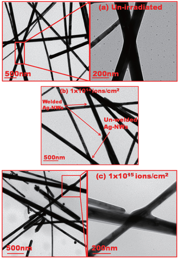
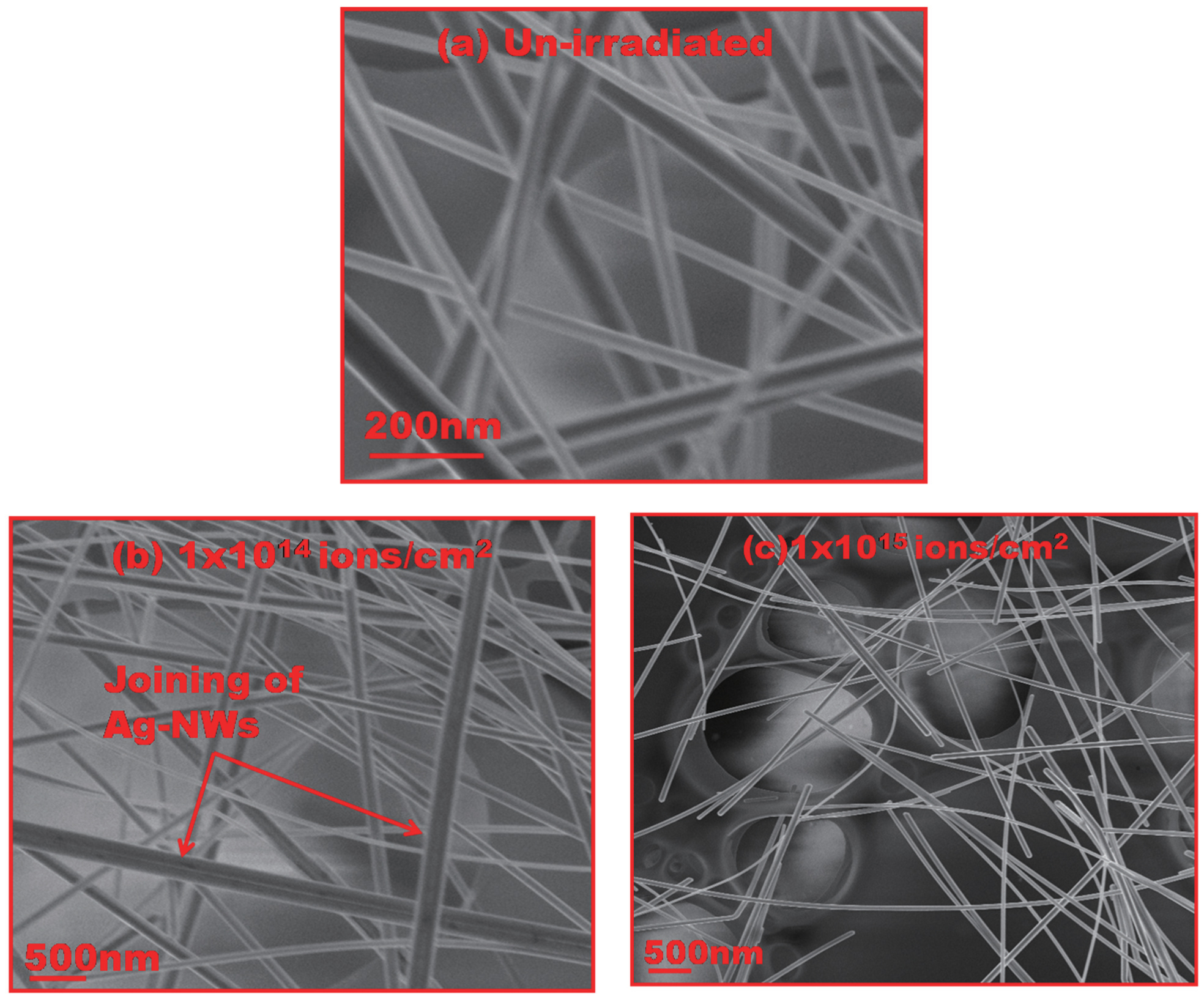
Figure 1(a) shows a typical TEM image of a random Ag-NW network before irradiation. The diameters of un-irradiated Ag-NWs range from 100 nm to 150 nm. The inset of Fig. 1(a) shows a high-resolution transmission electron microscope (HRTEM) image of a location where overlapping of Ag-NWs could be found in an X-shape before proton irradiation. TEM images in Figs. 1(b) and 1(c) show random networks of proton irradiated Ag-NWs with diameters in a range of 100 nm–200 nm at different fluences of MeV proton ions. The TEM image in Fig. 1(a) shows the un-welded Ag-NWs in a cylindrical shape before irradiation. However, after irradiation of these nanowires with proton beam, random network of well joined Ag-NWs is obtained and can be clearly seen in Figs. 1(b) and 1(c). Corresponding SEM images are shown in Figs. 2(a)–2(c).
Fig. 1. TEM images of a random network of Ag-NWs, respectively, without (a) being irradiated, where the inset shows the HRTEM image of Ag-NWs overlapped in an X-shape before irradiation, and with being irradiated at (b) 1 × 10¹⁴ ions/cm2 and (c) 1 × 10¹⁵ ions/cm2, where the inset shows the HRTEM image of Ag-NWs overlapped in an X-shape after irradiation.
Fig. 2. SEM images of random network of Ag-NWs without (a) and with being irradiated at (b) 1 × 10¹⁴ ions/cm2 and (c) 1 × 10¹⁵ ions/cm2, respectively.
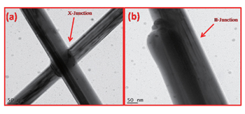
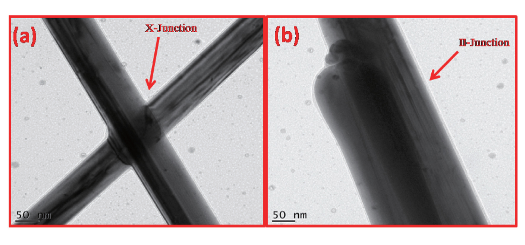
At an initial fluence of 1 × 10¹⁴ ions/cm2, Ag-NWs start to weld with each other in the forms of X-, II-, and V-shapes molecular junctions between Ag-NWs. However, this welding is fractional and can be seen in Fig. 1(b). At a fluence of 1 × 10¹⁵, perfect X-, II-, and V-shape molecular junctions between Ag-NWs are confirmed and ultimately become an optimum welded network due to H+ ion irradiation without distorting the morphology of nanowires. No slicing and cutting of Ag-NWs can be detected in respective SEM and TEM images. Figures 3(a) and 3(b) show Ag-NWs weld in an X-shape and II-shape respectively. HRTEM images of welded planes in X-, and II-shapes are shown in Figs. 3(b) and 3(c).
Fig. 3. TEM images of Ag-NWs irradiated at 1 × 10¹⁵ ions/cm2 welded in (a) X-shape and (b) II-shape; HRTEM images of (c) X-shape welded planes and (d) II-shape welded planes.
Interconnection between individual silver nanowires might be explained using the thermal spike model. For a faster beam of proton ions (⩾0.11 MeV), the kinetic energy of the ions is usually transferred to target electrons (electronic energy loss, Se) and for this reason Se may perhaps play an imperative role in the atomic transport process at the contact positions of individual Ag-NWs.[32]
When the energetic proton beam hits an individual Ag nanowire, ions might tend to lose a small fraction of their kinetic energy by columbic interaction with atomic electrons.[33] According to the thermal spike model, these excited electrons are in a thermodynamical equilibrium in a few 10−15 s through electron–electron interactions and discharge their energy to Ag lattice atoms by electron–phonon coupling in 10−13 s–10−10 s. This energy is then deposited to the Ag lattice probably along a proton track and results in localized spikes of heat produced, called thermal spikes. It might depend on the potency of electron–phonon coupling, the temperature along the proton path in the matter may significantly enhance the melting point of the silver material and a molten zone or a liquid cylinder of a few nm in depth is created at the interface of crossing regions between two Ag-NWs.[32] However, these molten phases at intersecting positions are transitory and are in several thousand of degree Kelvin, resulting in atomic displacement and mass transport of two Ag-NWs into each other exactly at crossing positions. In a picosecond time frame, proton tracks turn cold and results in the agglomeration of Ag-NWs atoms at crossing positions. For atomic displacement, the incident flux plays a major role at a given energy. With increasing incident flux, the localized heating effect of material increases and results in the mass transport of Ag-NW atoms into each other at contact position. So, these MeV proton induced thermal spikes are localized by nature and increase with increasing incident beam flux, causing Ag-NWs to weld with each other[34]
To avoid damage caused by surplus ion beam irradiation, we select middle-range ion energies, fluences, and room temperature to achieve welding of NWs and reduce the destructive effect because of excessive power simultaneously. During proton irradiation, if ion fluence is low, less heat is produced or a small number of defects would be generated in the crossing region between two Ag-NWs. Neither the amount of heat produced, nor restructured surface atom nor vacancy is adequate to make bonding between nanowires or to weld nanowires due to localized heat produced by ionization. If the ion dose is too high, surplus protons fluence will damage both interface regions and the body of Ag-NWs.[35]
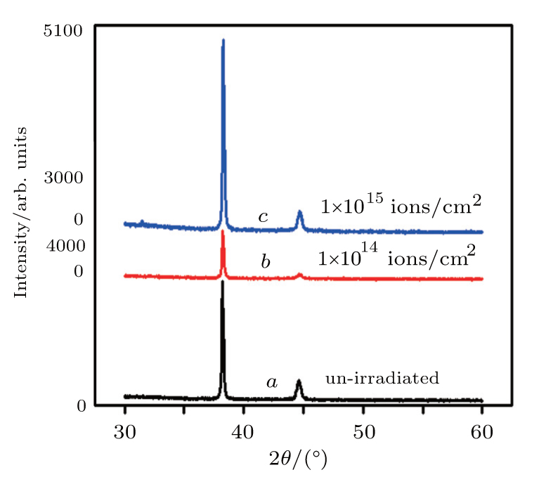
To confirm structural stabilities of Ag-NWs networks after H+ ion irradiation, XRD measurements are also performed at room temperature and are shown in Fig. 4.
Fig. 4. XRD spectra of random network of Ag-NWs without (a) and with being irradiated at (b) 1 × 10¹⁴ ions/cm2 and (c) 1 × 10¹⁵ ions/cm2.
The irradiation fluence of H+ ions is mentioned in each of the curves a, b, and c in Fig. 4. From Fig. 2, it can be seen that x-ray diffraction patterns of un-irradiated and H+ irradiated Ag-NWs networks exhibit peaks at 2θ angles corresponding to the associated planes of Ag-NWs face centered cubic structure (JCPDS Card No. 04-0783).[36] The sharpness of each of the diffraction peaks in all XRD patterns indicates the high crystallinity of its corresponding Ag-NW network before and after proton irradiation.
Moreover, it can be seen from Fig. 4, the XRD peak intensity corresponding to the (111) peak is found to decrease after the first fluence of H+ ions and then increase with the increase of irradiation fluence. This decrease in peak intensity after the initial fluence might be due to the production of irradiation induced point defects and/or defect clusters, which might cause the creation of some receptacles of amorphous regions and change the crystallinity of the material.[37] These irradiation-induced defects might be instigated due to a collision cascade effect and the sputtering of a considerable number of atoms from the Ag-NWs lattices.[38–41] Moreover, the TEM image of the respective Ag-NWs network (curve b in Fig. 4) irradiated at the first fluence of proton ions shows that the NW diameter has a slight decrease as compared with that of an un-irradiated Ag-NWs network, which might be a sign of the removal of atoms from Ag-NW lattices due to the interaction of H+ ions. However, the observed increase in peak intensity at high irradiation fluence (see curve c in Fig. 4) might indicate the improvement in crystallinity of Ag-NWs, which might be caused by the high defect recombination rate due to H+ ions induced thermal heating of the material, thus significantly reducing the amorphous regions in NW lattices.[41] Moreover, H+ induced heating can lead to a substantial drop in the defect number because of the migration of silver atoms, and an interstitial atom can migrate into a vacancy; and hence, fix both defects.[37] Hence a stable defect recoil atom should obtain energy greater than the threshold displacement energy of the atom in the material.[37] Therefore, at higher irradiation fluences, most of the energy deposition might be caused by electronic energy losses or ionization (as a result of columbic interaction of H+ ions and NWs atoms) rather than nuclear energy losses.
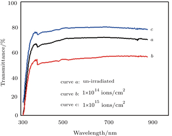
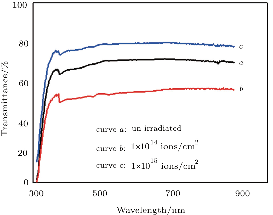
The optical properties of Ag-NW networks arise due to surface plasmonic resonance and are significantly different as compared with those of bulk silver. The optical transmittance spectra of Ag-NW networks are shown as curves a, b, and c in Fig. 5. As can be seen from curves a, b, and c in Fig. 5, spectra exhibit lower transmittance and strong absorption band (approximately 374 nm, which is in the ultraviolet region and might be due to the surface plasmonic resonance effect).[37,42,43] While sizes of wires decrease to nanoscale, the absorbance band comes into view in the ultraviolet region of UV-Visible spectra of Ag-NWs, however this band is missing in bulk silver.[43] This absorption band might appear due to an interaction of conduction electron with an electromagnetic field.
Fig. 5. Transmittance spectra of random network of Ag-NWs without (a) and with being irradiated at (b) 1 × 10¹⁴ ions/cm2 and (c) 1 × 10¹⁵ ions/cm2.
In fact, the interaction of the electromagnetic field with Ag-NW network induces an oscillating electric field and this oscillating electric field agitates the conduction electrons at the surface, as a consequence, the electron cloud displaces with respect to the nuclei. The electron cloud oscillates with respect to the nuclei due to the columbic force of attraction between electrons and material nuclei.[43] Collective oscillations of conduction band electrons at the surface are called surface plasmonic resonance.[43] This resonance is accountable for the decreased transmittance, enhanced scattering and absorption of light in the UV region. In the case of metal nanowires, these surface plasmonic bands lead to highly tunable and controllable properties which can be exploited in various applications. Moreover, it can be seen from Fig. 5 that transmittances of presented networks decrease initially with the first fluence of H+ ions which might be due to defects induced by the collision cascade effect. The transmittances of Ag-NW networks irradiated at a higher fluence of H+ ions are found to increase, which might be due to the improvement in the crystal quality of respective Ag-NW networks at the higher fluence of H+ ions.
4. Conclusions
We successfully fabricate large scale Ag-NW networks by H+ ion beam irradiation. These large scale networks of Ag-NW are realized by H+ ion-induced thermal spikes, which leads to the production of molten zones and transport of mass material through these zones at intersecting positions of nanowires and leads to the welding of nanowires at intersecting positions. The changes in optical transparency and structure of the Ag-NW networks caused by H+ ion irradiation are also studied. An improvement in optical transparency is also observed after H+ ion irradiation. Thermal spikes induced by H+ ion beam irradiation are a successful approach to reducing the wire-wire contact resistance for the large scale fabrication of robust and highly transparent networks.


 , S Naseem1, ‡,