


Radiation-induced 1/f noise degradation of PNP bipolar junction transistors at different dose rates
[Zhao Qi-Feng1, Zhuang Yi-Qi1, Bao Jun-Lin1, †,  , Hu Wei2]
, Hu Wei2]


† Corresponding author. E-mail:
Project supported by the National Natural Science Foundation of China (Grant Nos. 61076101 and 61204092).
It is found that ionizing-radiation can lead to the base current and the 1/f noise degradations in PNP bipolar junction transistors. In this paper, it is suggested that the surface of the space charge region of the emitter-base junction is the main source of the base surface 1/f noise. A model is developed which identifies the parameters and describes their interactive contributions to the recombination current at the surface of the space charge region. Based on the theory of carrier number fluctuation and the model of surface recombination current, a 1/f noise model is developed. This model suggests that 1/f noise degradations are the result of the accumulation of oxide-trapped charges and interface states. Combining models of ELDRS, this model can explain the reason why the 1/f noise degradation is more severe at a low dose rate than at a high dose rate. The radiations were performed in a Co60 source up to a total dose of 700 Gy(Si). The low dose rate was 0.001 Gy(Si)/s and the high dose rate was 0.1 Gy(Si)/s. The model accords well with the experimental results.
The PNP bipolar junction transistors are utilized in analog IC applications such as input stages, active loads, and current sources. Owing to surface effects, some types of PNP bipolar junction transistors are known to exhibit extreme sensitivities to ionizing radiation.[1] For many current bipolar linear technologies, the primary failure mechanism is the reduction of the current gain.[2–4] In 1991, it was found that bipolar junction transistors may exhibit the enhanced low dose rate sensitivity (ELDRS).[5] Since its initial report, all aspects concerning this effect (mechanism, modeling, testing, and recently studied ELDRS) has comprehensively been analyzed.[6–17] However, most of the radiation studies of Si bipolar junction transistors reported so far have mainly focused on experimental results about the radiation-induced changes in the measured electrical characteristics of the devices. To the authors’ knowledge, very little data regarding 1/f noise performance degradation with the total dose and the dose rate have been reported for Si bipolar junction transistors.[18,19]
The total dose 1/f noise performances of PNP bipolar junction transistors radiated at different dose rates are presented. Based on the theory of carrier number fluctuation, a model is developed which identifies the physical mechanism responsible for the 1/f noise degradation. The model suggests that the 1/f noise degradations can be attributed to the accumulation of oxide-trapped charges and interface states. Combining models of ELDRS, the 1/f model can explain the reason why the 1/f noise degradation is more severe at a low dose rate than at a high dose rate. This work utilizes experiments and an analytical model to explain the mechanism responsible for radiation-induced 1/f noise degradation.
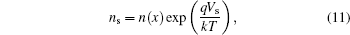
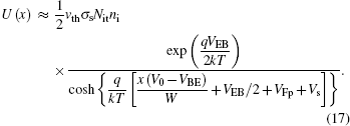
When the base- emitter is under forward bias, the difference in quasi-Fermi energy level between electrons ɛFn and holes ɛFp is related to the voltage VEB applied to the Base-Emitter junction, that is, ɛFn − ɛFp = qVEB,[20] where q is the electron charge. The carrier concentrations in the space charge region are given by


The origin of the x axis is at the edge of the space charge region on the p side as shown in Fig.

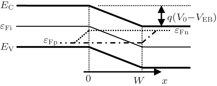 | Fig. 1. Energy level of p–n junction under forward bias. |
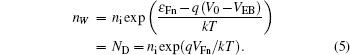
At x = 0, the hole concentration is given by
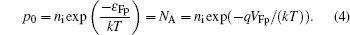
At x = W, the electron concentration is given by
From Eq. (

From Eq. (

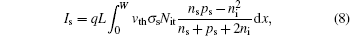
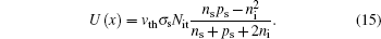
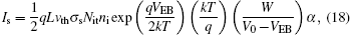
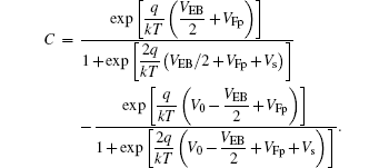
In most analytical treatments of recombination in the space charge region, the spatial dependence is neglected;[4] instead, it is usually assumed that the total recombination rate can be obtained from the behavior of the peak recombination rate. However, in a radiated polar junction transistor, this assumption is subject to important limitations.[21] It is necessary to include the recombination current throughout the surface of the space charge region of the emitter-base junction to adequately describe the effects of radiation. The recombination current at the surface of the space charge region may be calculated by integrating the recombination rate over the surface of the emitter-base space charge region. It can be given by
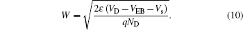
For a PNP bipolar junction transistor, an oxide-trapped charge causes the surface region of an n-type base to fall into accumulation. As the base is usually in accumulation mode, the following correlation between the surface potential Vs and oxide-trapped charge Not is valid:[22]

We assume that the surface potential at the surface of the space charge region is approximately equal to the surface potential at the surface of the base. The surface potential would make the potential at the surface of the space charge region bend. At the same time, the accumulation of the base forces a reduction in the width of the space charge region at the surface as shown in Fig.
 | Fig. 2. Cross-section of the emitter base junction, illustrating accumulation regions in the presence of positive oxide charge. |
The carrier concentrations at the surface of the space charge region can be given by


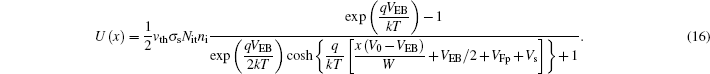
Assuming VBE > 4kT/q, equation (

The opposing nature of oxide charge and interface traps may be verified with the aid of Fig.
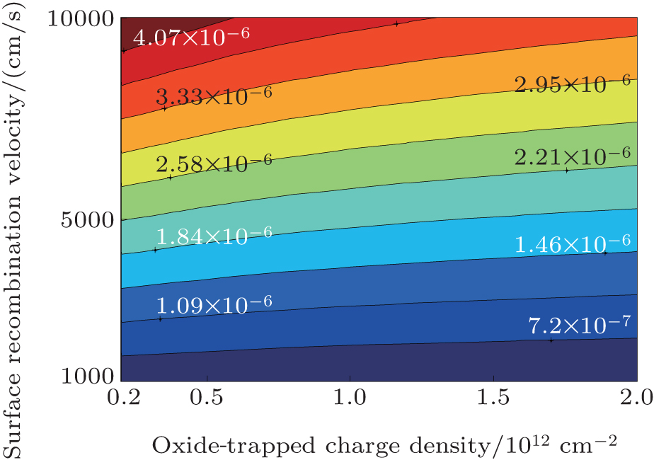 | Fig. 3. Contour plots of base surface current response to an interactive combination of surface recombination velocity and oxide charge density. |
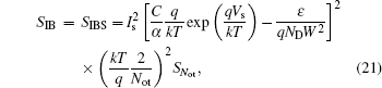
The low frequency 1/f noise in a bipolar junction transistor is currently explained by the fluctuations in carrier number[23–25] or Hooge Mobility.[26,27] It is generally admitted that the variation of power law exponent α of the current noise with the dc current provides the information about the noise type. When the exponent α is close to unity, the Hooge mobility fluctuations are believed to be responsible for the low frequency noise, while α ≈ 2 is indicative of carrier number fluctuations. Several 1/f noise models of a bipolar junction transistor were introduced in detail in Ref. [28]. For a bipolar junction transistor, the base current fluctuations are decomposed into surface and volume originated noise sources.[29] Often the surface 1/f noise component is the dominant component of the base 1/f noise.[30]
Experimentally, 1/f spectra have been observed in one or more tens of frequency ranges, requiring a process characterized by a time constant distributed over a wide range. Based on the theory of carrier number fluctuation,[31] there are two classes of carrier traps near the Si–SiO2 interface, that is, oxide-trapped charges and interface states. The interface states exchange carriers with the conduction band or valence band of silicon as the generation-recombination centers due the SRH process, and, only a definite time constant is observed for interface states at a given energy. The oxide-trapped charge can exchange the carrier with the conduction band or valence band of silicon through the trap-tunneling process. The interface states are distinguished from the oxide-trapped charges by their location, thus by their shorter relaxation time constant than those of the oxide-trapped charges. Therefore the interface states contribute to relatively high frequency components of noise compared with the oxide-trapped charges whose time constants are longer than those of the interface states and have a wide range of time constants, which are necessary to generate a 1/f noise spectrum. So, the base surface 1/f noise of a PNP bipolar junction transistor may be ascribed to the low frequency fluctuations in the surface recombination current due to the dynamic trapping–detrapping of carriers into oxide-trapped charges.
The dynamic trapping–detrapping of carriers into oxide-trapped charges causes an oxide-trapped charge fluctuation δNot, which should lead to a base surface current fluctuation δIs. According to Eq. (

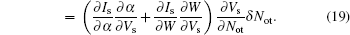
Combining Eqs. (

According to Eq. (

As the energy distribution of oxide-trapped charges is now not completely determined,[32] we make a simplified assumption that Not(E) is uniformly distributed over the whole energy range, and expressed as


Combining Eqs. (
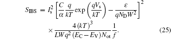
Equation (
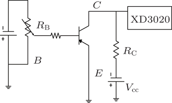
The devices studied in this work were vertical PNP bipolar junction transistors obtained from a semiconductor manufacturer in China. Each device had an emitter with a doping surface of 1 × 1020 cm−3, and the base doping is 1 × 1017 cm−3. All transistors were irradiated with ionizing gamma-radiation from a Co60 source at room temperature. The low dose rate was 0.001 Gy(Si)/s and the high dose rate was 0.1 Gy(Si)/s. The parameters of the transistors were measured prior to and after 100, 300, 500, and 700 Gy(Si) of total dose exposure. The measured electrical parameters were the base current IB and the collector current IC, which were measured by an HP4156 Semiconductor Parameter Analyzer. The common emitter configuration circuit was used for noise measurements as shown in Fig.
 | Fig. 4. Circuit used to bias the transistor for noise measurements. |
The relative change in the base current, ΔI/I0, is plotted versus total dose in Fig.
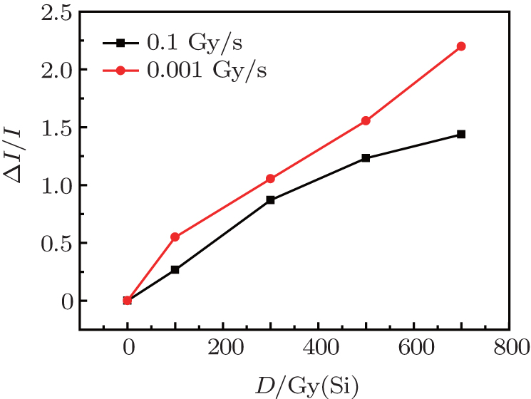 | Fig. 5. Normalized base currents versus total dose. |
Figures
 | Fig. 6. Base current noise spectra versus total doses of (a) 0.1 Gy(Si)/s and (b) 0.01 Gy (Si)/s. |
The power spectral density of the base current is commonly expressed as follows:

From Eqs. (

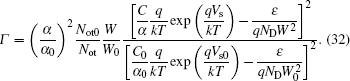
The amplitude of 1/f noise B is used to evaluate the base current noise degradation. The relative change of B can be written as
From Eq. (
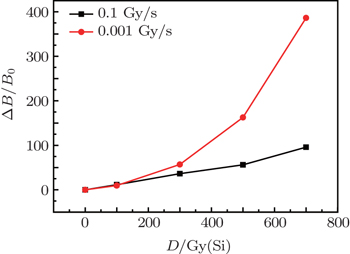
The plots of relative change in the amplitude of 1/f noise, ΔB/B0, versus absorbed dose under radiations at two dose rates are shown in Fig.
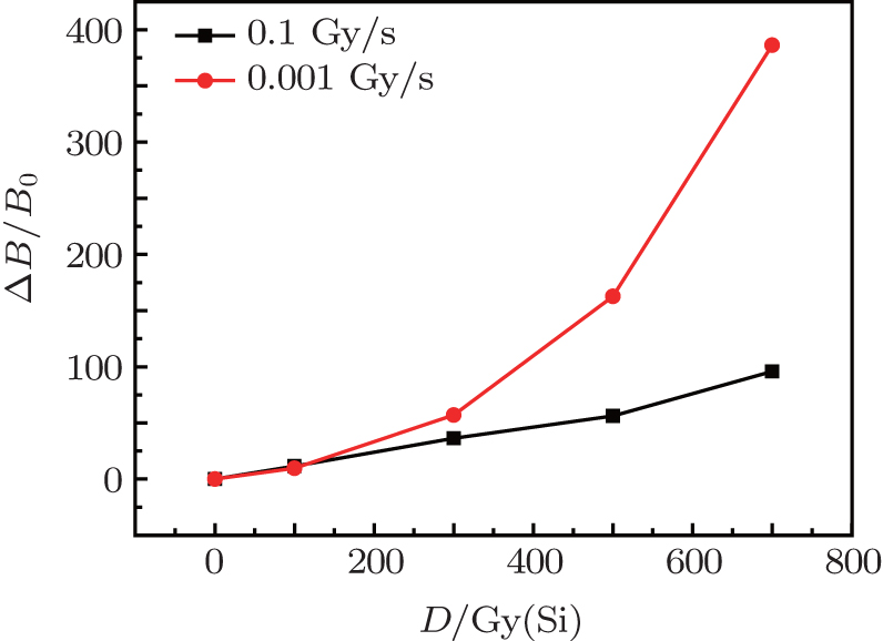 | Fig. 7. Normalized amplitude of 1/f noise, ΔB/B0, versus total dose. |
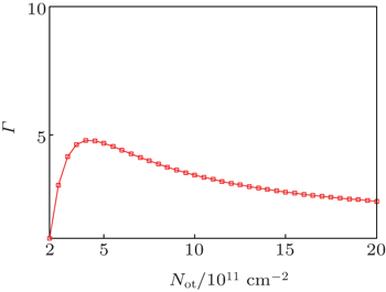
Let
Figure
 | Fig. 8. Γ as a function of oxide-trapped charge density Not. |
The increase of base current noise spectrum SIB with dose augment can be explained as follows. With the accumulation of total dose, the oxide-trapped charges and the interface states increase. Firstly, according to Eq. (
Many models have been presented to explain ELDRS in a linear bipolar transistor. These models may be grouped into three main categories[35]: 1) space charge models,[36–40] 2) bimolecular process models,[41–46] and 3) a binary reaction rate model.[47] The phenomenon that at the same total dose level ΔI/I0 the ΔB/B0 changes faster at the dose rate of 0.001 Gy(Si)/s than at the dose rate of 0.1 Gy (Si)/s, can be explained with these models. According to these models, more interface states and oxide-trapped charges are induced at the low dose rate, which leads to more severe degradations of the base current and the base 1/f noise at the low dose rate.
In this paper, it is suggested that the surface of the space charge region of the emitter-base junction is the main source of the base surface 1/f noise for a PNP bipolar junction transistor with a heavily doped emitter. Based on the theory of carrier number fluctuation and the model of base surface recombination current, a 1/f noise model is developed, which can be used to explain the 1/f noise degradation induced by the radiation. Combining the models of ELDRS, this model can explain the fact that the 1/f noise is more severe at a low dose rate than at a high dose rate. The essential point of this work is to qualitatively describe the radiation-induced 1/f noise degradations of PNP bipolar transistors. Although many important aspects of the problem are neglected, the presented model may be helpful for understanding some of the features of bipolar radiation response.
| 1 | |
| 2 | |
| 3 | |
| 4 | |
| 5 | |
| 6 | |
| 7 | |
| 8 | |
| 9 | |
| 10 | |
| 11 | |
| 12 | |
| 13 | |
| 14 | |
| 15 | |
| 16 | |
| 17 | |
| 18 | |
| 19 | |
| 20 | |
| 21 | |
| 22 | |
| 23 | |
| 24 | |
| 25 | |
| 26 | |
| 27 | |
| 28 | |
| 29 | |
| 30 | |
| 31 | |
| 32 | |
| 33 | |
| 34 | |
| 35 | |
| 36 | |
| 37 | |
| 38 | |
| 39 | |
| 40 | |
| 41 | |
| 42 | |
| 43 | |
| 44 | |
| 45 | |
| 46 | |
| 47 |