Li Tian-Tian, Yang Tie, Fang Jia, Zhang De-Kun, Sun Jian, Wei Chang-Chun, Xu Sheng-Zhi, Wang Guang-Cai, Liu Cai-Chi, Zhao Ying, Zhang Xiao-Dan. Microstructure and lateral conductivity control of hydrogenated nanocrystalline silicon oxide and its application in a-Si:H/a-SiGe:H tandem solar cells. Chinese Physics B, 2016, 25(4): 046101
Permissions
Microstructure and lateral conductivity control of hydrogenated nanocrystalline silicon oxide and its application in a-Si:H/a-SiGe:H tandem solar cells
Li Tian-Tian1, 2, 4, 5, Yang Tie1, 3, Fang Jia1, 2, 4, 5, Zhang De-Kun1, 2, 4, 5, Sun Jian1, 2, 4, 5, Wei Chang-Chun1, 2, 4, 5, Xu Sheng-Zhi1, 2, 4, 5, Wang Guang-Cai1, 2, 4, 5, Liu Cai-Chi3, Zhao Ying1, Zhang Xiao-Dan1, 2, 4, 5, †,
Institute of Photo-electronic Thin Film Device and Technique, Nankai University, Tianjin 300071, China
Collaborative Innovation Center of Chemical Science and Engineering (Tianjin), Tianjin 300072, China
School of Material Science and Engineering, Hebei University of Technology, Tianjin 300130, China
Key Laboratory of Photo-electronic Thin Film Devices and Technology of Tianjin, Tianjin 300071, China
Key Laboratory of Photo-electronic Information Science and Technology of Ministry of Education, Nankai University, Tianjin 300071, China
Project supported by the Hi-Tech Research and Development Program of China (Grant No. 2013AA050302), the National Natural Science Foundation of China (Grant No. 61474065), Tianjin Municipal Research Key Program of Application Foundation and Advanced Technology, China (Grant No. 15JCZDJC31300), the Key Project in the Science & Technology Pillar Program of Jiangsu Province, China (Grant No. BE2014147-3), and the Specialized Research Fund for the Ph. D. Program of Higher Education, China (Grant No. 20120031110039).
Abstract
Abstract
Phosphorous-doped hydrogenated nanocrystalline silicon oxide (n-nc-SiOx:H) films are prepared via radio frequency plasma enhanced chemical vapor deposition (RF-PECVD). Increasing deposition power during n-nc-SiOx:H film growth process can enhance the formation of nanocrystalline and obtain a uniform microstructure of n-nc-SiOx:H film. In addition, in 20s interval before increasing the deposition power, high density small grains are formed in amorphous SiOx matrix with higher crystalline volume fraction (Ic) and have a lower lateral conductivity. This uniform microstructure indicates that the higher Ic can leads to better vertical conductivity, lower refractive index, wider optical band-gap. It improves the back reflection in a-Si:H/a-SiGe:H tandem solar cells acting as an n-nc-SiOx:H back reflector prepared by the gradient power during deposition. Compared with the sample with SiOx back reflector, with a constant power used in deposition process, the sample with gradient power SiOx back reflector can enhance the total short-circuit current density (Jsc) and the initial efficiency of a-Si:H/a-SiGe:H tandem solar cells by 8.3% and 15.5%, respectively.
Thin film solar cells, especially silicon-based, provide a highly potential alternative for the massive demand of photovoltaic modules, and a lot of efforts are made to increase their stable efficiencies. Among many factors, light management and cell structure play critical roles in improving cell performance.[1,2] During recent years, nanocrystalline silicon oxide (nc-SiOx:H) films with low absorption and low refractive index have been successfully prepared and used as key functional layers in thin-film silicon solar cells. For instance, this film has been proposed to be used as a window layer in n or p-side illuminated silicon solar cells,[3–7] the a-Si:H solar cell efficiency reaches up to 10.2%. The intermediate reflector (IR) in multi-junction solar cells achieved 13.6% efficiency of a-Si:H/nc-Si:H tandem solar cell.[8–14] For the back reflector (BR) in thin-film silicon solar cells,[13–16] and an extra thin resistive layer or alternative n-layer,[11,15] an above 11% of efficiency of a-Si:H/a-SiGe tandem solar cells has been achieved. The doped nc-SiOx:H film is a mixed phase material which has an oxygen rich amorphous silicon oxide (a-SiOx:H) phase and a doped nanocrystalline silicon (nc-Si:H) phase.[16,17] Consequently, its optical band gap (E04), which is defined as the photon energy gap at which the absorption coefficient α equals 1 × 104 cm−1, and refractive index can be precisely tuned by the O-content inside the a-SiOx:H phase. Therefore, the doped nc-SiOx:H film combined with a suitable conductivity as p-type or n-type doped nanocrystalline silicon (nc-Si:H) phase can serve as a replacement for the conventional doped layers in thin-film silicon tandem solar cells to enhance both the optical and electrical properties. In addition, to achieve highly stable efficiency, two or more junction tandem solar cells with interlayer between sub-cells are necessary, where SiOx material was also employed and also showed a better result than ZnO.[14,18] Consequently, the preparation of a doped nc-SiOx:H film, which has wider optical band-gap, lower refractive index, and higher conductivity, is a key process to improve the performances of thin-film silicon tandem solar cells. The microstructure of a doped nc-SiOx:H film is a very important factor that can regulate these characteristics, and many deposition parameters also control the structure, such as deposition power and hydrogen dilution.[10,12]
In this study, we report on such a material development for n-type nc-SiOx:H (n-nc-SiOx:H) films and focus on the deposition power as a crucial parameter in the radio frequency plasma enhanced chemical vapor deposition (RF-PECVD). In comparison with conventional SiOx material fabricated in a fixed deposition power, an optimized structure is proposed by introducing gradient deposition power with or without interval time in an n-nc-SiOx:H film deposition process. Finally, this optimized structure of n-nc-SiOx:H film is successfully used in a-Si:H/a-SiGe:H tandem solar cells as a BR and the results show its great enhancement over cell performance.
2. Experimental details
The n-nc-SiOx:H films were prepared in a PECVD multi chamber system using an excitation frequency of 13.56 MHz on Corning Eagle XG glass substrates with a temperature of approximately 190 °C. The process gases used were carbon dioxide (CO2), hydrogen (H2), and 10% silane (SiH4) diluted in H2, and phosphine (PH3) as n-type dopant source. Deposition parameters such as H2 dilution (H2-fiow/SiH4-flow), doping concentration (PH3-flow/SiH4-flow) and chamber pressure were fixed to be 68.7, 3%, and 85 Pa, respectively. The power was varied during the deposition to control the optical and electrical properties. The details can be seen in Table 1.
Table 1.
Table 1.
Table 1.
Deposition parameters of n-nc-SiOx:H films and the solar cell samples which use corresponding films.
.
Sample film/solar cell
CO2/SiH4 gas flow ratio
Power/W
Deposition time/min
Growth condition
A/SC1
20
45
B/SC2
30
45
C/SC3
40
45
D/SC4
50
45
continuous
E/SC5
1.3/1.2
60
45
30
25
F/SC6
40
20
30
25
20 second
G/SC7
40
20
interval
Table 1.
Deposition parameters of n-nc-SiOx:H films and the solar cell samples which use corresponding films.
.
The structural, electrical, and optical properties of the films were investigated by Raman spectroscopy (λ = 488 nm), scanning electron microscopy (SEM), dark conductivity measurements, and optical transmission spectrum. To evaluate the properties of n-nc-SiOx:H films, mass-produced level amorphous silicon/amorphous silicon–germanium (a-Si:H/a-SiGe:H) double junction tandem solar cells were selected as reference devices.
The crystalline volume fraction of the film was probed by Renishaw via Raman reflex spectrometer using the 488-nm line of an Ar laser. The dark conductivity (σd) was measured by using coplanar Al-electrode at 300 K, which characterizes the lateral conductivity, and the film thickness was measured by surface step profilometer. Optical transmission spectra were obtained by using Cary spectrophotometer. The morphology of the n-nc-SiOx:H film surface at the tandem solar cells was achieved by scanning electron microscopy (SEM). The photovoltaic parameters of the solar cells, which were all patterned to an area of 0.25 cm2, were measured under standard test condition (STC): AM1.5G, 300 K and 100 mW/cm2, and the external quantum efficiency (EQE) was also calculated from the spectral response measured.
3. Results and discussion
3.1. Microstructural properties
The Raman scattering spectra are de-convoluted into two Gaussian-shaped peaks: (i) the transverse optical (TO) mode of the a-SiOx:H phase (centered around 480 cm−1) and (ii) the TO vibrational mode of the nc-Si:H phase (centered around 520 cm−1).[19] The crystalline volume fraction of the n-nc-SiOx:H film is defined as the Raman intensity ratio Ic which is equal to the ratio of the integrated area of the nc-Si:H peak to the total peak area (a-SiOx:H + nc-Si:H) as given in the following equation:
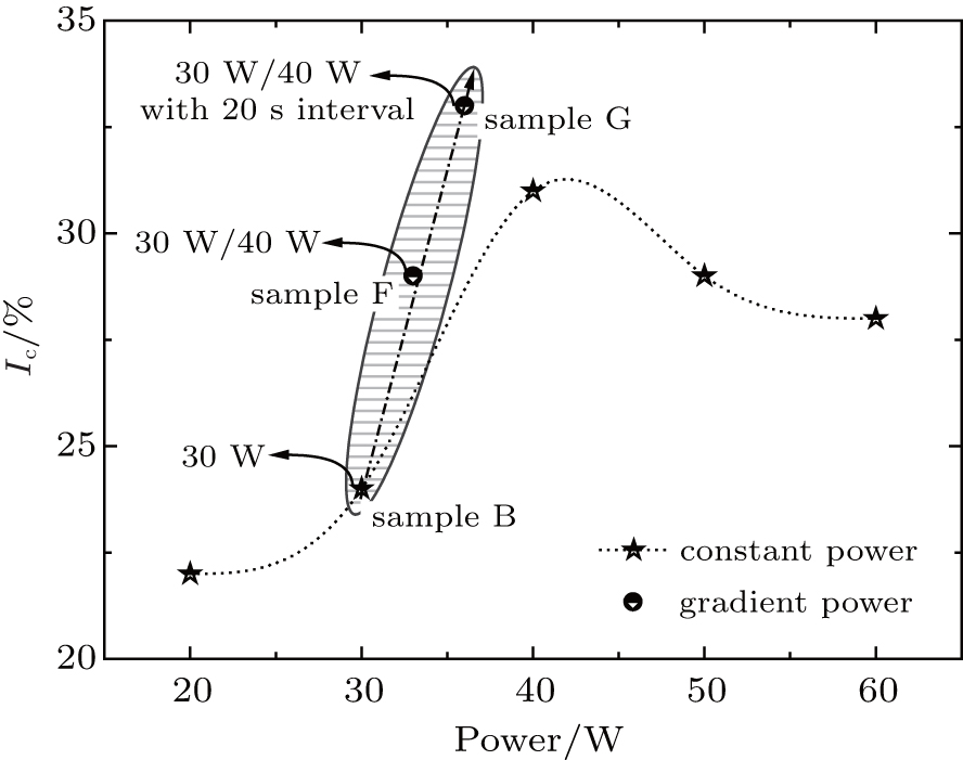
Figure 1 shows the variations of Ic (calculated from Eq. (1)) with deposition power for the n-nc-SiOx:H films: the Ic increases from 22% to 31% with the power increasing up to 40 W because of the etching effect of H. However, when the power is higher than 40 W, the Ic decreases to 28% because of the inhibitory action of forming Si–Si network in nanocrystalline. The increasing power enhances the dissociation of CO2 to assist the O to form Si–O amorphous phase rather than Si–Si. And when the gradient power is introduced to grow the n-nc-SiOx:H, the Ic is improved from 24% to 33% significantly. So the microstructure of the n-nc-SiOx:H film with gradient power should be further studied.
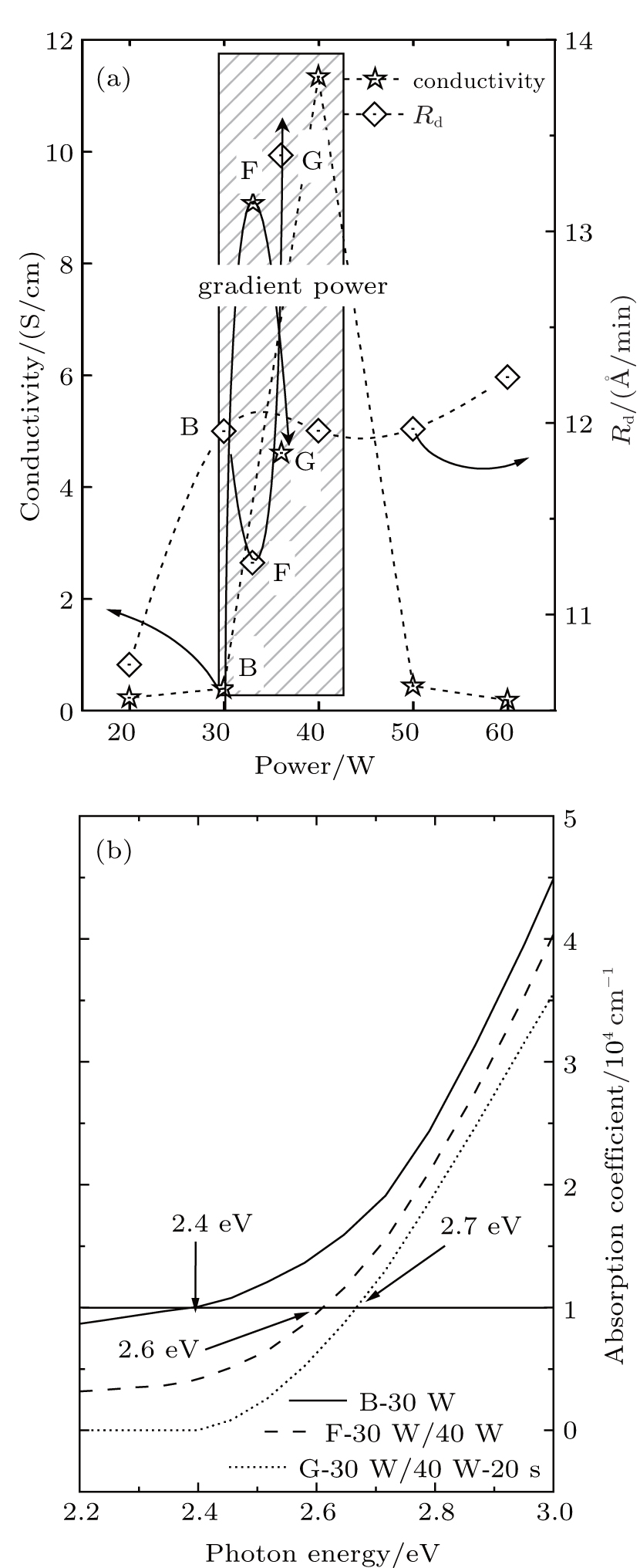
Fig. 1. Plots of Ic versus deposition power for n-nc-SiOx:H films.
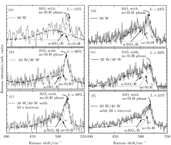
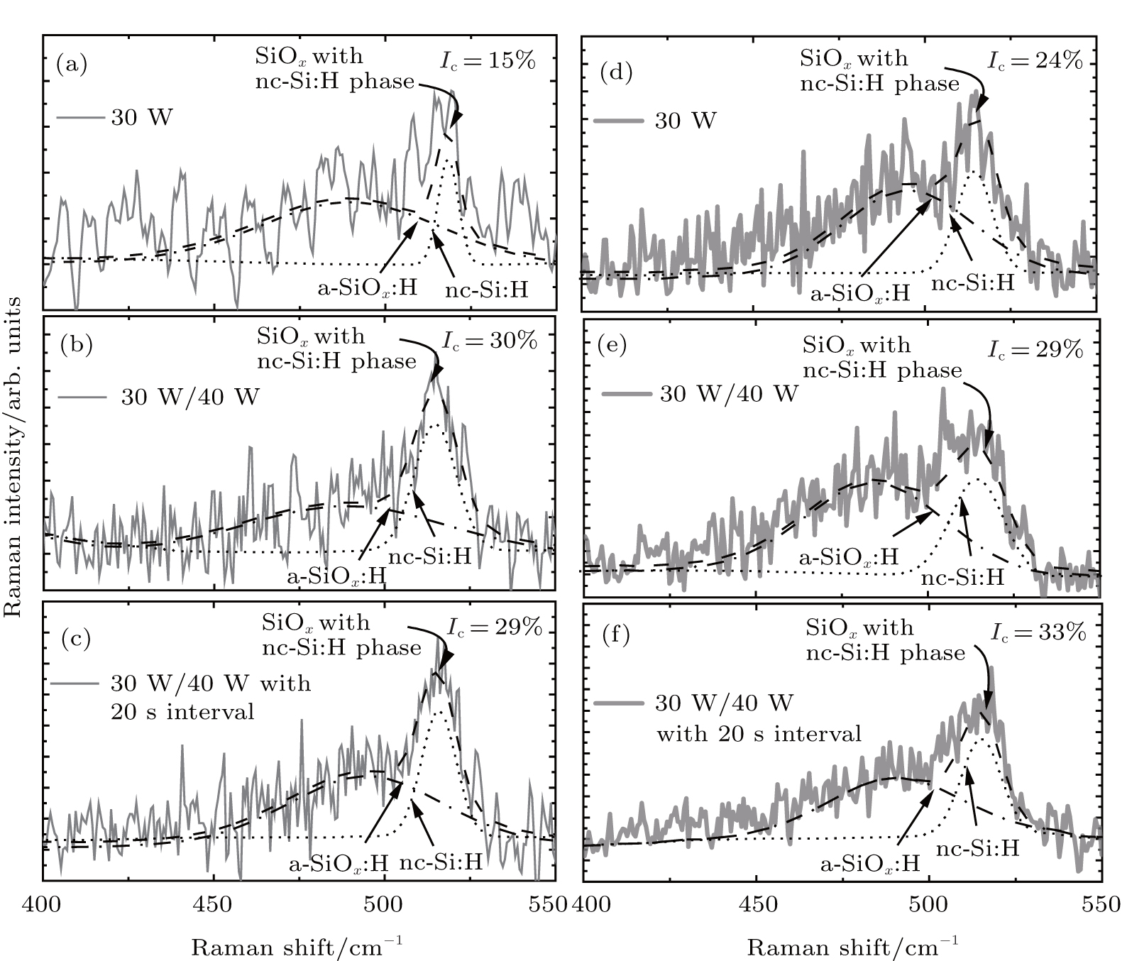
Figure 2 shows the corresponding peaks and the Ic profiles of samples B, F, and G. Double-side incident method is used to investigate the mixing uniformity of n-nc-SiOx:H films in the vertical direction.
Fig. 2. Raman spectra of the n-nc-SiOx:H films with the laser incidence from ((a), (b), and (c)) the glass side (samples B, F, G) and ((d), (e), and (f)) from film side (samples B, F, G), respectively.
From the Raman spectra shown in Figs. 2(a) and 2(d), the n-nc-SiOx:H material grown under constant power is not uniform, and the crystalline volume fraction Ic = 15% (from glass side) increases up to 24% (from film side) in the growth direction. Figures 2(b) and 2(e) shows that by increasing power in the deposition process, the crystallinity volume fraction increases (approximately 30%) with power increasing, and the n-nc-SiOx:H material becomes more uniform. On the one hand, high power produces more H atoms and it would achieve higher energy in the plasma to break the weak Si–Si bond to rebuild ordered structure. On the other hand, high power also enhances the dissociation efficiency of CO2,[12] and the O content changes the a-SiOx:H phase proportion in n-nc-SiOx:H film. These two processes are both existent during the deposition, and the H-etch effect dominantly affects the results. In addition, the 20-s interval during power change is favorable because of the highest crystallinity of 33% (Figs. 2(c) and 2(f)). A proposed explanation for this observation involves the changing deposition power between two different n-nc-SiOx:H structures, higher power leading to higher crystallinity, and an interval that can make the pre-growth film relaxed sufficiently and microstructures get a steady-state condition. The new-forming layer can be beneficial to the later crystallization. The residual stress is calculated by Wolf’s empirical formula [20] and shown in Fig. 3.
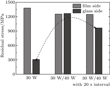
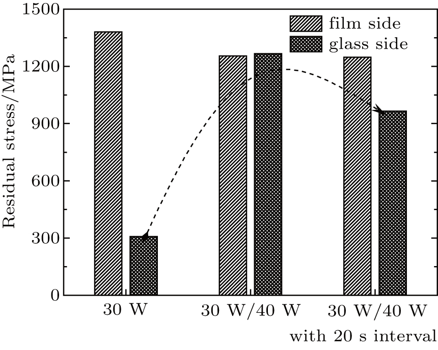
Fig. 3. Variations of residual stress of the deposited n-nc-SiOx:H films with power from film side and glass side, respectively.
It is evident from Fig. 3 that the low Ic has a lowest residual stress of 308 Mpa from glass-side at 30 W and with Ic increasing during the film growth, the residual stress increases up to 1380 Mpa. The Si–Si network in a-SiOx phase can increase the residual stress in the film, and the 20-s interval helps relax strained Si–Si network in a-SiOx phase and the residual stress drops from 1250 Mpa to 965 Mpa from glass-side.
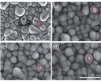
Figure 4 shows the surface morphologies of the n-nc-SiOx:H films deposited on the a-Si:H/a-SiGe:H tandem solar cells. Compared with the solar cell without SiOx BR in Fig. 4(a), the solar cells fabricated with the n-nc-SiOx:H BR keep the column-growth mode from the cell substrate. Distinctly, in the n-nc-SiOx:H column there are two separate phases — small grains scattered throughout in the uniform matrix and indicated separately by the circle and arrow in Fig. 4. In Figs. 4(b) and 4(c) corresponding to the cells with different n-nc-SiOx:H BRs (sample B and sample F). The diminished grains are distributed more uniformly, meaning that more O atoms are incorporated into the material since the gradient deposition power is introduced. Moreover, 20-s interval during power change which improves the crystallinity, can lead to the smaller grains and higher density (Fig. 4(d), sample G). Generally, the crystallinity volume fractions and mixing uniformities of the n-nc-SiOx:H films have all been improved by increasing deposition power in the growth process.
Fig. 4. SEM images of a-Si:H/a-SiGe:H solar cell with different n-nc-SiOx:H layers as BR. Panel (a) shows the case without SiOx back reflector, and panels (b)–(d) show the cases corresponding to samples B, F, and G.
3.2. Laterally electrical and optical properties
The oxygen-rich region in n-nc-SiOx:H film, totally amorphous, supplies low refractive index and high band gap because of incorporated oxygen;[21] the n-doped nanocrystalline silicon region provides sufficient electrical conductivity.[22,23] The influences of deposition parameters on lateral conductivity and growth rate are presented in Fig. 5(a). The average deposition rates are little enhanced from 11 Å/min to 13 Å/min with the increase of deposition power. But the lateral conductivities of all n-nc-SiOx:H layers are greatly different. Increasing power will assist the dissociation of SiH4 to enhance the deposition rate, and the H-etching effect can also promote the formation of nanocrystalline silicon which has high doping efficiency to achieve a high lateral conductivity up to 11.3 S/cm when the power is at 40 W. But with power increasing further, the increase of CO2 dissociation reduces the nanocrystalline phase in n-nc-SiOx:H film, which leads a decrease of lateral conductivity. Furthermore, due to the non-uniformity of the crystallinity in the growth direction, amorphous incubation layer is formed during the early stage of the n-nc-SiOx:H layer deposition and lower H-etching effect leads to the low crystallinity volume fraction with poor lateral conductivity (0.4 S/cm) under the condition of constant deposition power of 30 W. Increasing power in the deposition process can improve the crystallinity volume fraction and increase the lateral conductivity up to 9.1 S/cm. However, when the 20-s interval is introduced in the deposition process before increasing power, the lateral conductivity drops from 9.1 S/cm to 4.6 S/cm. Figure 4(d) shows that the crystalline grains which have smaller sizes and higher density distributed in uniformly amorphous phase (red circled) and more grain boundaries become potential energy barriers to restrict the thermally activated transport of carriers.[24]
Fig. 5. Average deposition rate (Rd) and lateral conductivity (a), absorption coefficient and n, k (b) of the different n-nc-SiOx:H films.
The optical properties of the n-nc-SiOx:H films are also studied. Figure 5(b) presents the absorption coefficient α, the index of refraction n, and the extinction coefficient k (inset graph), which are obtained by calculating transmission spectra.[25] It is obvious that absorption coefficient α of the film fabricated by increasing the power during deposition process is reduced and the optical gap E04 is increased from 2.4 eV to 2.6 eV. Increasing power causes more CO2 to decompose and higher O content of the n-nc-SiOx:H film to increase its optical gap.[21,26] Besides, it is also found in Fig. 5(b) that 20-s interval during power change increases the E04 slightly (2.7 eV). We have mentioned that the sample G have more grain boundaries, and this highly disordered grain boundary region becomes poly-hydride bonding configuration which mades it likely exhibit higher optical gap.[27–,30] Furthermore, higher O content could also reduce the n from 3.2 to 2.9 (at 1000 nm), and it would introduce the refractive gradient between the above layers, thereby increasing the light-trapping effect of solar cells.
3.3. Solar cells performance
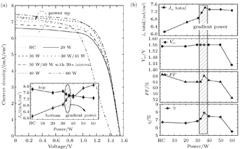
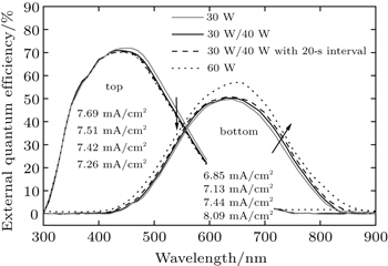
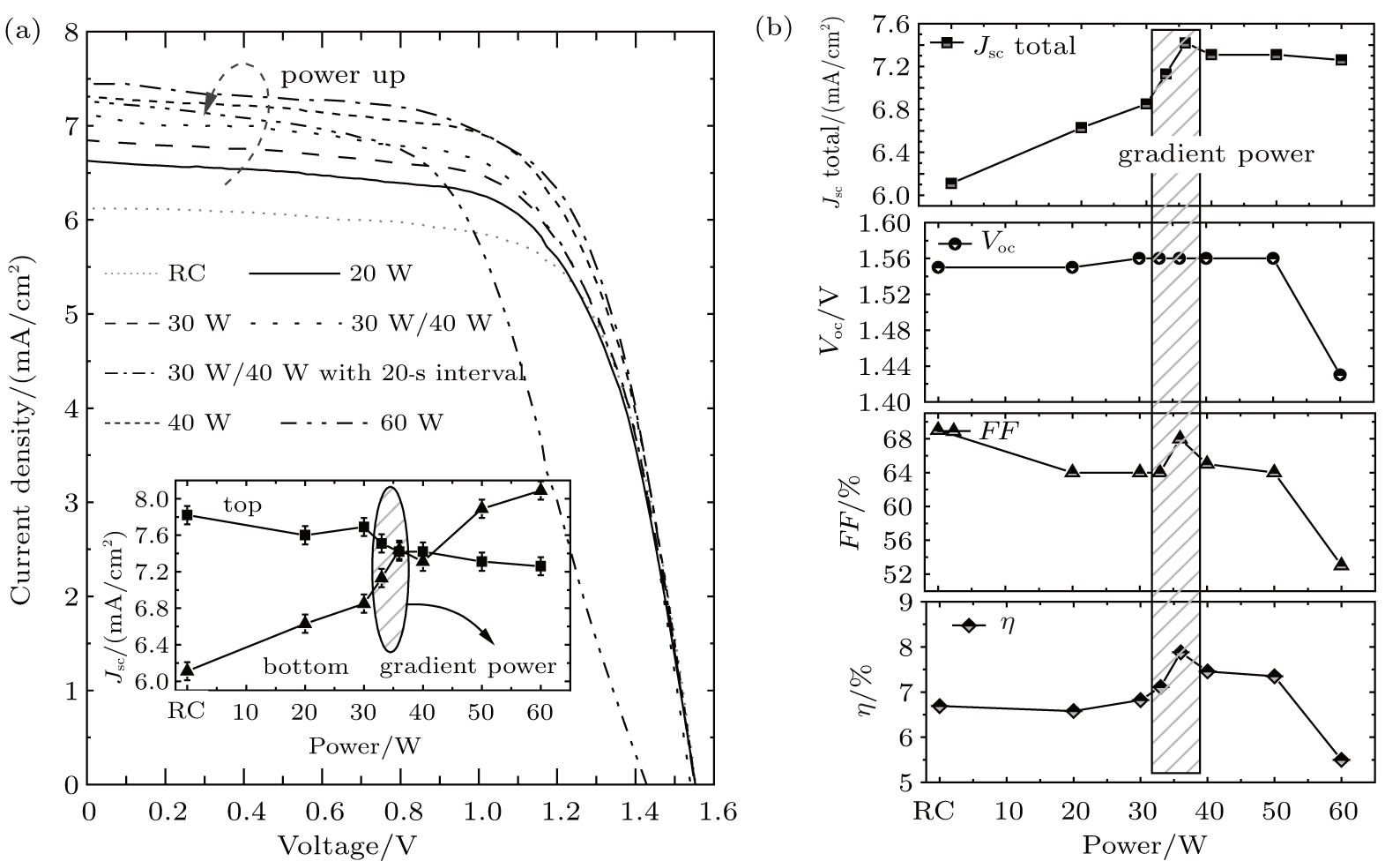
Figure 6(a) shows the J–V curves of n-nc-SiOx:H films serving as BRs in a-Si:H/a-SiGe:H solar cells. It is found in Fig. 6(b) that the short circuit current density (Jsc) of the cells increases significantly when using n-nc-SiOx:H materials as BR (reference cell without SiOx BR, sample RC). The open circuit voltage (Voc) decreases rapidly from 1.56 V to 1.43 V when the deposition power reaches as high as 60 W because of electrically-shielded effect of carriers at i/n interface with high O content n-nc-SiOx:H film. The comparison of the optimized SiOx BR (gradient deposition power with 20-s interval) with the standard SiOx BR (constant deposition power) shows that the Jsc is enhanced largely (6.85 mA/cm2 to 7.42 mA/cm2), maximally reaching up to 8.3%. As a consequence, the cell efficiency increases from 6.82% to 7.88% with a relative increase of 15.5%. By observing the change trend of fill factor (FF), the results show that the n-nc-SiOx:H film which has the highest lateral conductivity is not suitable for the a-Si:H/a-SiGe:H solar cell (FF = 65%). Because the highest lateral conductivity can collect more local current drains, which relate to the weak diodes and shunts, FF of solar cell decreases. The 20-s interval is beneficial to the solar cells because it has high FF (FF = 68%). The small grains with highest density form high potential energy barrier to prevent the collection of local current drains, thus increasing FF of solar cell. However, because of the electrically-shielded effect of carriers, the increase of series resistance (Rs) causes the FF to reduce significantly when the deposition power of n-nc-SiOx:H film is as high as 60 W.
Fig. 6. (a) J–V curves of solar cells, the inset showing the top cell and bottom cell’s Jsc tendency, and (b) the parameters of the solar cell.
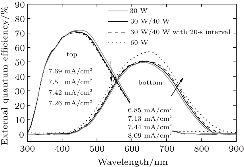
The variations of external quantum efficiency (EQE) of a tandem cell with wavelength for different n-nc-SiOx:H serving as BRs are shown in Fig. 7. The optimized n-nc-SiOx:H layer used as BR affects both bottom and top cell: the spectrum response in the whole wavelength region of bottom cells is improved, especially in the long wave-length region from 650 nm to 850 nm; the top cell spectrum response slightly reduces in the range from 500 nm to 750 nm because this part of light is utilized by the bottom cell fabricated with additional n-nc-SiOx:H layer. This corresponds to the top cell Jsc dropping from 7.69 mA/cm2 to 7.26 mA/cm2 and the bottom cell Jsc rising from 6.85 mA/cm2 to 8.09 mA/cm2 (see the inset in Fig. 6(a)). The refractive index step between the absorbing layer and n-nc-SiOx:H layer leading to the reflection of light at interface increases the optical light path in the absorbing layer,[22] and this mainly affects the long wavelength part corresponding to the bottom cell. Moreover, the 20-s interval during changing deposition power in sample SC7 shows its better performance than sample SC6 because of higher refractive index step. But with the deposition power of nc-SiOx:H film further increasing from 40 W to 60 W, the bottom cell Jsc begins to increase and becomes higher than top cell Jsc (see the inset in Fig. 6(a)), which causes the Jsc of tandem solar cells to decrease. So by using the optimized n-nc-SiOx:H as BR, a better current matching between top and bottom cell is obtained.
Fig. 7. Plots of external quantum efficiency versus wavelength of a-Si:H/a-SiGe:H solar cells with different SiOx back reflector.
4. Conclusions
In the present work, each of n-nc-SiOx:H films prepared under a gradient deposition power is used as a back reflector in a-Si:H/a-SiGe:H solar cell. Based on the Raman and SEM results, the crystallinity volume fraction increases (approximately 33%) with gradient power increasing in a n-nc-SiOx:H film deposition process. Because the etching effect of H atoms is larger than the dissociation efficiency of CO2, the mixing uniformity of n-nc-SiOx:H film is improved. The dark conductivity confirms that increasing deposition power in the deposition process of n-nc-SiOx:H film raises the lateral conductivity considerably (from 0.4 S/cm to 9.1 S/cm) and the higher dissociation efficiency of CO2 leads to the lower α, n, and k. In addition, the lowest α, n, and k of the n-nc-SiOx:H film are obtained by 20-s interval before power change. The lateral conductivity of film drops to 4.6 S/cm for the higher potential energy. The Jsc of a-Si: H/a-SiGe:H solar cell with this optimized SiOx BR increases from 6.85 mA/cm2 to 7.42 mA/cm2, because the higher refractive index step enhances the light trapping of the long wavelength in the absorbing layer and then improves the cell efficiency. In conclusion, this n-nc-SiOx:H film with proper optical properties and optimized lateral conductivity improves the performance of the a-Si:H/a-SiGe:H solar cell significantly.
Microstructure and lateral conductivity control of hydrogenated nanocrystalline silicon oxide and its application in a-Si:H/a-SiGe:H tandem solar cells


 ]
]