Strip silicon waveguide for code synchronization in all-optical analog-to-digital conversion based on a lumped time-delay compensation scheme
1. IntroductionAn analog-to-digital converter (ADC) is an important part of a communication system which needs to satisfy the requirements for the rapid development of ultra-wide-band applications such as an advanced radar system, high speed optical communication, etc.[1–3] The electrical ADC whose sample rate and art resolution are several giga-samples per second (GSa/s) and 10 bit respectively cannot meet the requirements for ultra-wide-band applications because of its inherent electrical bottle-neck such as clock jitter and sampling aperture, etc.[1–4] The all-optical ADC has attracted much attention because it can overcome the limitation of electronic devices, and meanwhile achieve appropriate quantization resolution and sampling rates. Optical quantization could be realized by soliton self-frequency shift (SSFS), higher-order soliton fission, cross-phase modulation effects, etc.[5–13] Optical quantization utilizing the SSFS effect is a promising option among the above schemes because of its ultrafast response speed, which can realize the sampling rate transparency. The outstanding results in analog-to-digital conversion were given based on the SSFS effect.[14–20] In the process of frequency shift, time-delays between optical pulses with different peak powers occur inherently, leading to the non-synchronization of the quantized optical pulses and coding error. The multiple optical time-delay lines (TDLs) are utilized to compensate for time-delay in the previous schemes whose disadvantages are complicated and expensive. Meanwhile, they cannot meet the demands of miniaturization and photonic integration. Silicon photonic technology is suitable for photonic integration, owing to its compatibility with the complementary metal–oxide–semiconductor (CMOS) process. The optical waves can be confined into the sub-micron region by the high refractive index of silicon by using the silicon-on-insulator (SOI) technology.[21] Some SOI signal processing schemes have been proposed,[22–28] but to the best of our knowledge, there is still no report on an all-optical ADC. The strip waveguide structure on the order of centimeters in length allows for a stronger negative dispersion than conventional fiber and photonic crystal fiber (PCF). However, the organic material requires a non-CMOS process and strict temperature limitation, which renders it unsuitable for mass-manufacturing.[29,30]
In this paper, we propose a lumped time-delay compensation scheme with 2-bit quantization resolution to realize optical pulse synchronization for the first time by inserting a strip silicon waveguide instead of the multiple optical TDLs after the SSFS module. The time-delays between quantized pulses with different peak powers at the output of the silicon wavelength are compensated for. Results based on numerical simulation are discussed.
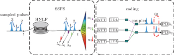
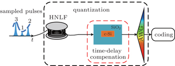
2. Principle of operationFigure 1 shows an all-optical ADC with 2-bit quantization resolution whose two primary modules are all-optical quantization and coding based on the SSFS effect and optical interconnection, respectively. In Fig. 1, the discrete sampled optical pulses, which can be generated by the four-wave mixing (FWM) effect, are delivered into a span of highly nonlinear fiber (HNLF) to realize a power-to-wavelength conversion based on the SSFS effect. At the output of HNLF, the central wavelength of the spectrum presents a red shift and the shift value is directly proportional to the peak power of the input optical pulse, therefore an arrayed waveguide grating (AWG) is utilized to separate different central wavelengths. Optical signals with different central wavelengths are sent to the specific ports of the AWG and then they are delivered into a coding module. The optical interconnection is realized by using several attenuators, TDLs and photodiodes (PDs) in the coding module. The expressions of outputs b1 and b2 are

By utilizing the optical interconnection, 4 optical pulses (including a pulse with a peak power of 0) are converted into 2-bit Gray codes at outputs of PDs, while the magnitude of the frequency shift corresponds to a Gray code encoding.
All-optical quantization is achieved by the SSFS effect, the central wavelength of the optical pulse presents a red shift. Meanwhile, the optical pulse has a time-delay at the output of the HNLF. The dynamic transmission of sampled optical pulses in HNLF can be described by the simplified generalized nonlinear Schrodinger equation (GNLSE). Solving the GNLSE with the moment method, the time-delay of the sampled pulse Δt can be obtained as follows:[31,32]

where Δ
Ω is the frequency shift of the sampled pulse,
β2 and
L are the second-order dispersion coefficient and the length of fiber, respectively. The dispersion parameter
D = −2
πcβ2/
λ2,
λc and
λ0 are the central wavelengths of the quantized pulse and initial pulse, respectively. When the dispersion parameter
D and the fiber length
L are constants, the time-delay Δ
t is directly proportional to
λc from Eq. (
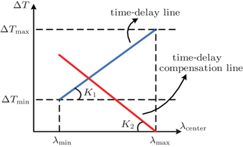
2). According to the relation between the time-delay and the central wavelength after the SSFS effect, the compensation mechanism is shown in Fig.
2. The blue and red lines represent the time-delay and time-delay compensation curves with slopes of
K1 and
K2, respectively. In order to compensate for the time-delay, the relation
K2 = −
K1 = (Δ
Tmax − Δ
Tmin)/(
λmax −
λmin) needs satisfying, while
Dc =
K2/
Lc. Here,
Dc and
Lc are the dispersion parameter and the length of the lumped time-delay compensation device.
3. Waveguides design and time-delay compensation performanceThere are many different ways to realize time-delay compensation as long as the red line can be achieved in Fig. 2, e.g., dispersion compensating fiber (DCF), large dispersion PCF. The group-velocity dispersion (GVD) has a dispersion length  where T0 is the initial pulse width and β2 is the GVD coefficient. The self-phase modulation has nonlinear length LNL = (γP0)−1, where γ is the nonlinear parameter and P0 is the initial peak power. The dispersion plays a major role, while the nonlinearity is relatively weak, requiring L ≪ LNL and L ≈ LD, for waveguide length L.
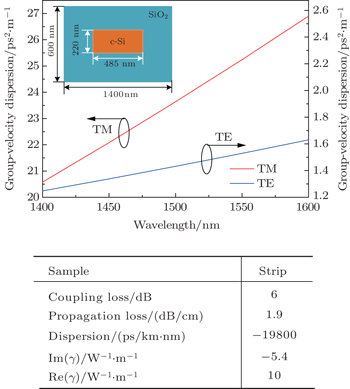
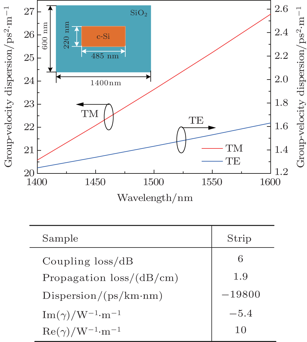
Fortunately, the tight mode confinement in an SOI waveguide helps introduce significant waveguide dispersion and thus allows one to obtain a dramatically large normal group-velocity dispersion. In other words, a large and flattened negative dispersion parameter is obtained by designing the SOI waveguide appropriately.[33–38] Figure 3 shows the calculated GVD curves for our waveguide. For dimensions of 1400 nm×600 nm and an etching dimension of 485 nm×220 nm (see the inset of Fig. 3). The other parameters of the strip silicon waveguide are shown in the upper right part of Fig. 3. Based on the waveguide structure, the fundamental TM mode exhibits a GVD of 25.24 ps2/m and a dispersion of –19800 ps/(km·nm) at 1550 nm. Meanwhile, the dispersion variation is ±0.5 ps/(km·nm) from 1400 nm to 1600 nm. This value is 1000 times larger than that of standard silica fiber (β2 < 0.02 ps2/m). With such a high dispersion, the length of the strip silicon waveguide is shorter than that of the conventional fiber or PCF.
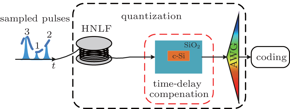
The lumped time-delay compensation scheme is shown in Fig. 4. Comparing Fig. 4 with Fig. 1, the time-delay compensation is inserted between the quantization module and the coding module. The strip silicon waveguide is brought forward from the HNLF and AWG to realize lumped time-delay compensation rather than multiple TDLs. The improvements are definitely useful for the integration and miniaturization of the all-optical ADC. The dynamic of an optical pulse inside a silicon waveguide is governed by the modified GNLSE, which includes the effects of two-photo absorption (TPA), free-carrier absorption (FCA), and free-carrier dispersion (FCD). The GNLSE is given by
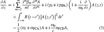
where
A is the slowly varying envelope,
βm is the
m-th dispersion coefficient,
γ0 and
γTPA are the real and imaginary part of the complex nonlinear coefficient,
ω0 is the center angular frequency of the optical pulse,
αl is the linear loss of the silicon waveguide,
αFCA and
nFCD are the coefficients of FCA and FCD, which are given by

and

with
λ0 and
λref being the input center wavelength and the reference wavelength,
Nc being the free-carrier density and given by

where
βTPA is the TPA parameter,
h is the Plank constant,
f0 is the center frequency,
Aeff is the effective mode field area of the silicon waveguide, and
τ is the effective carrier lifetime.
The nonlinear response function R(t) in Eq. (3) is related to the Raman contribution, and it is defined as R(t) = (1 − fR) δ (t) + fRhR (t), with fR being the fractional contribution of the nuclei to the total nonlinear polarization. The Raman response function hR (t) can be deduced from the Raman response spectrum. The Fourier transform HR (Ω) of hR (t) is given by

where
ΩR and
ΓR are the Raman shift and the bandwidth of the Raman gain spectrum at room temperature.
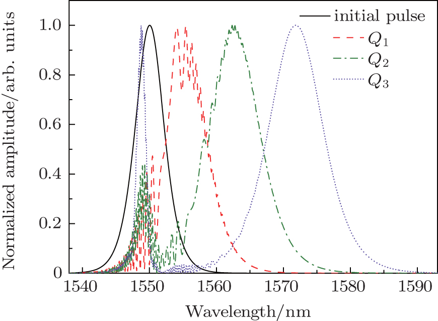
4. Simulation and discussionSolving the GNLSE with the split-step-Fourier method,[31] the dynamic behaviors of the pulses in the time and frequency domain in the quantization process is numerically analyzed. In Fig. 4, a string of hyperbolic secant optical pulses as sampled optical pulses with 0.53 ps full width at half maximum (FWHM), 40-GHz repetition rate and 1550-nm central wavelength is fed into a span of HNLF to present SSFS. To simulate the sampled pulses with different peak powers, a variable optical attenuation (VOA) is used to generate the sampled pulses with different powers. For example, the peak powers Q1, Q2, and Q3 of the sampled pulses are 9.58 W, 12.80 W, and 13.99 W, respectively. Q0 with a peak power of 0 is of no use in the coding module, so it is neglected in our simulation. After transmitting in a span of HNLF (γHNLF = 16 W−1·km−1, DHNLF = +3 ps/(nm·km), αHNLF = 0.9 dB/km) for SSFS, the central wavelengths of the sampled pulses are shifted to specific positions. The spectral profiles of the optical pulses Q1–Q3 after the HNLF are shown in Fig. 5. The magnitude of the central wavelength shift is in direct proportion to the peak power of the sampled pulse. As shown in Fig. 5, the optical signal is quantized after transmission through the HNLF. It is seen that the spectrum becomes overlapped with each other, which leads to the cross-talk between adjacent channels. Fortunately, the overlap points are all not higher than the FWHM level of the spectrum so that the cross-talk issue can be mitigated with the power equalization by the attenuator array and comparator decision.
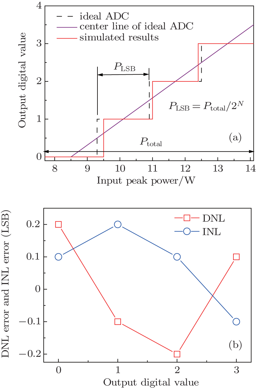
Figure 6(a) shows the transfer function of the 2-bit AOADC and figure 6(b) shows the differential nonlinear (DNL) and the integral nonlinear (INL) errors calculated from the transfer function, respectively. The transfer function increases monotonically without missing codes. As shown in Fig. 6(a), the least significant bit (LSB) power PLSB and the full-scale of the power range Ptotal are 1.6 W and 6.4 W, respectively. Meanwhile, a peak DNL error of 0.2 LSB and a maximum INL error of 0.2 are obtained.
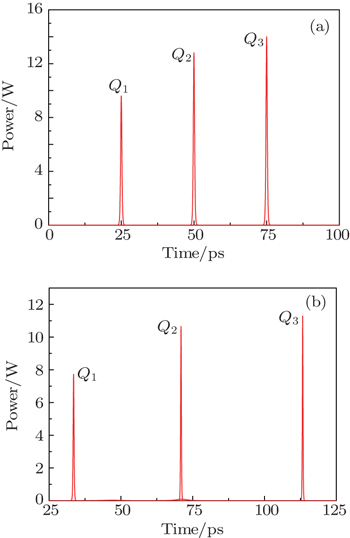
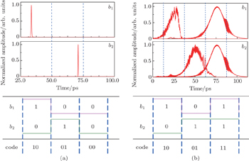
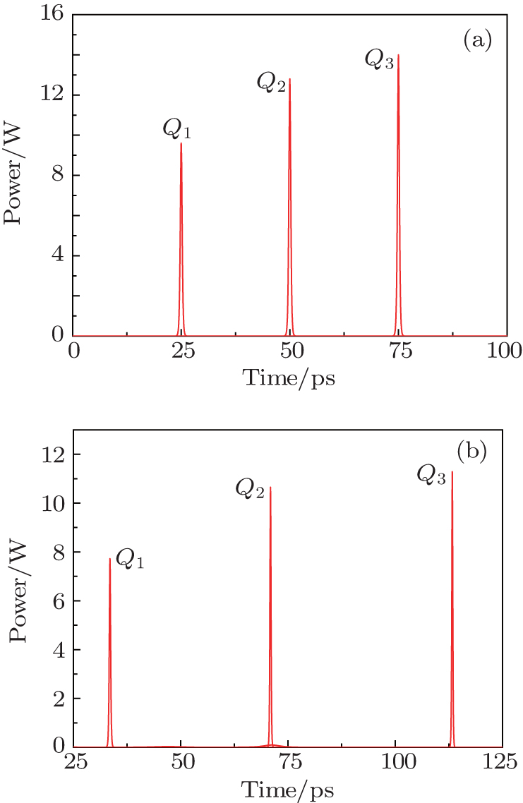
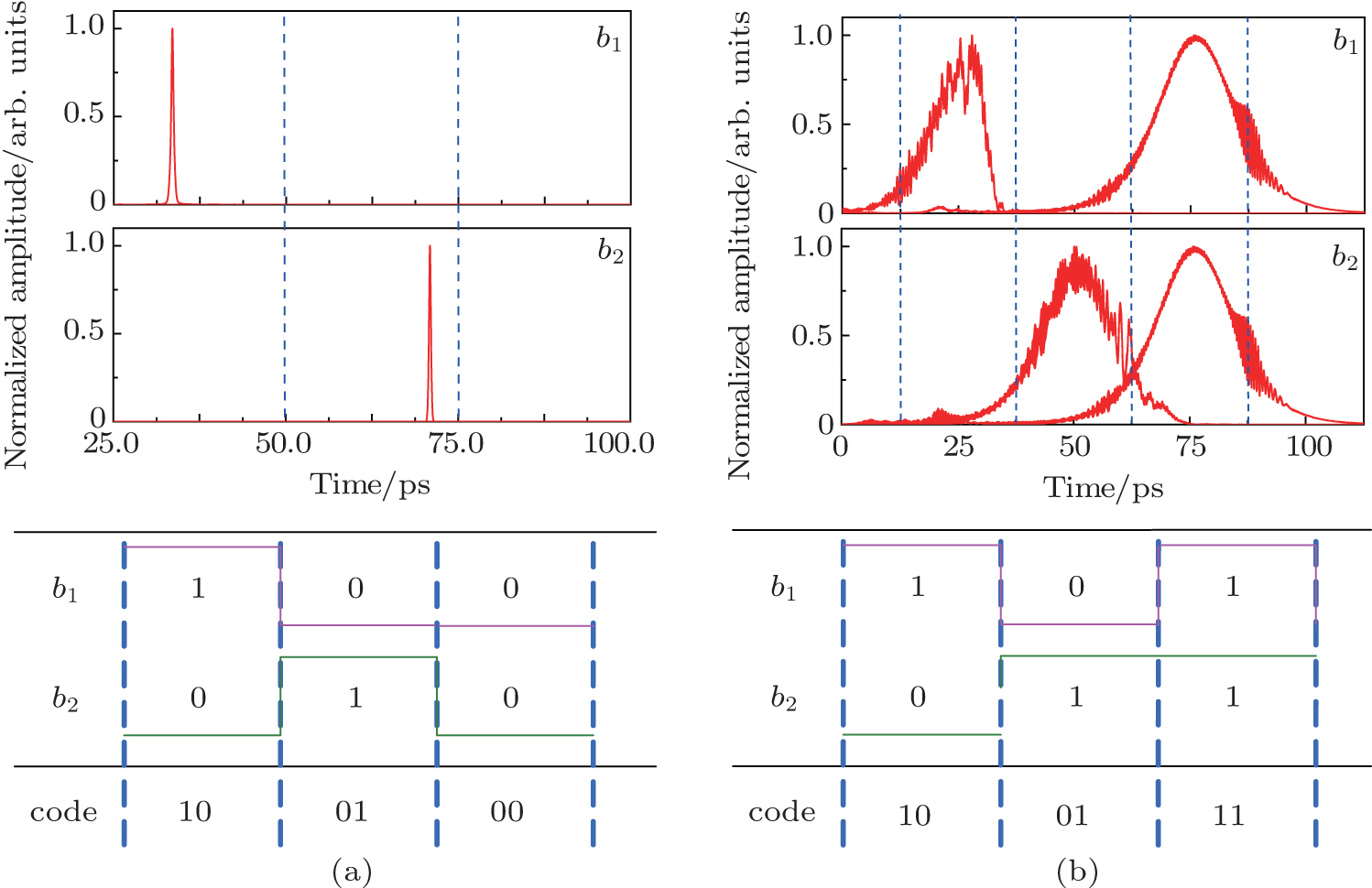
The initial sampled pulses are recorded in Fig. 7(a). The initial time interval of the adjacent pulses is 25 ps when the sampling rate is 40 GSa/s. The temporal profiles of the sampled pulses are recorded at the output of the highly nonlinear fiber (HNLF) in Fig. 7(b). After the quantization based on the soliton self-frequency shift (SSFS) effect, the sampled optical pulses with different peak powers have different time-delays. The coding error will be caused by the nonsynchronous issue in the final decision. Adjusting the bandwidth of AWG, the temporal profiles of PD detection and the coding results with time-delay are displayed in Fig. 8(a). Since the input optical pulses are “Q1, Q2, and Q3”, the correct codes should be “10 01 11”. However, as shown in Fig. 8(a), the coding results are “10 01 00” and the corresponding optical pulses become “Q1, Q2, and Q0”, which are inconsistent with the input ones. So the time-delay compensation is quite necessary for ensuring the coding correctness.
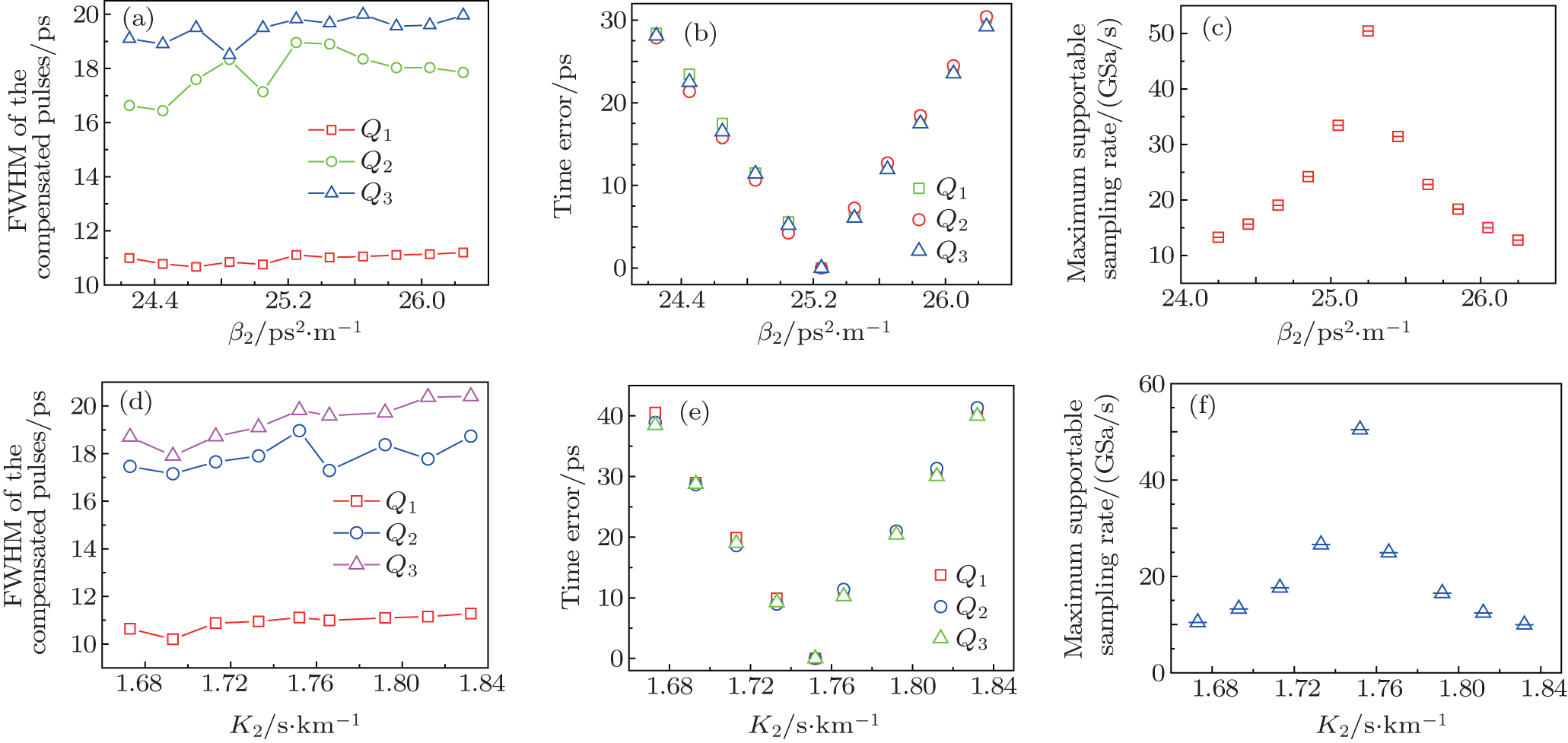
Here, a strip silicon waveguide is utilized to realize lumped time-delay compensation. As shown in Fig. 2, the slope of the time-delay curve is K1 = 1.752 ps/nm in the scheme. Thus, the slope of the time-delay compensation curve is K2 = −1.752 ps/nm. The strip silicon waveguide can be fabricated, starting from SOI wafers patterned with deep-UV lithography, which is a mature technique at present. In Fig. 8(b), the correct binary codes can be obtained based on the lumped time-delay compensation scheme. Because of the large GVD effect, however, the optical pulses after the silicon waveguide are simultaneously broadened. The pulse broadening effect can affect the maximum supportable sampling rate (MSSR) that is defined as

where the time-error is the magnitude of the difference between the time position of the compensated pulse and the one of the input pulses, and FWHM
broadened is the FWHM of the broadened pulses, respectively. From Eq. (
6), time-error and FWHM
broadened are both directly proportional to the reciprocal of the sampling rate. Considering the cases with the GVD fluctuation, the effect of
β2 on the FWHM of the compensated pulses is shown in Fig.
9(a). With the increase of
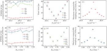
β2, the FWHM values of the three compensated pulses present fluctuations. However, the variations are relatively slight, which are all less than 2.52 ps. For example, the FWHM of
Q2 is 16.44 ps at the GVD value of 24.44 ps
2/m, and it is 18.96 ps at the GVD value of 25.24 ps
2/m; their difference is only 2.52 ps. In Fig.
9(b), the curve of the time error versus GVD is recorded. The interference of the sampled pulses will occur when the time error is not neglected. With the increase of
β2,
Q1,
Q2, and
Q3 have almost the same time error, and the maximum is 30 ps at the GVD value of 26.24 ps
2/m. Considering both the pulse broadening and GVD fluctuation issues, the curve of MSSR versus GVD is shown in Fig.
9(c) according to Eq. (
6). For example, the FWHM of the compensated pulses is 19.82 ps while GVD is 25.24 ps
2/m and the maximum central wavelength is 1572 nm in our scheme, and the sampling rate should be no more than 50.45 GSa/s. With the increase or decrease of GVD relative to 25.24 ps
2/m, the MSSR decreases due to the large dispersion of the strip silicon waveguide.
For the cases where the values of slope K2 are different, while the dispersion of the silicon waveguide remains constant and the length of the silicon waveguide is changed, the diagram of FWHM, time error and MSSR versus slope K2 are shown in Figs. 9(d), 9(e), and 9(f), respectively. In our scheme, the FWHMs of the compensated pulses are all slightly fluctuated with the variation of the parameter of the strip silicon waveguide, while the time errors all have relatively large variations correspondingly. The MSSR is mainly determined by the time error in the system based on the strip silicon waveguide. However, the base-order soliton case (0.5 < N < 1.4) is met by a VOA before the SSFS module; the effect from the nonlinearity of the silicon waveguide can be neglected.
The quantization resolution N is defined as
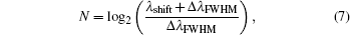
where
λshift and Δ
λFWHM are the magnitude of the center wavelength shift and the spectral width of the optical pulse at the output of HNLF. It is obvious that to obtain a large resolution
N, a larger
λshift and a smaller Δ
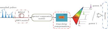
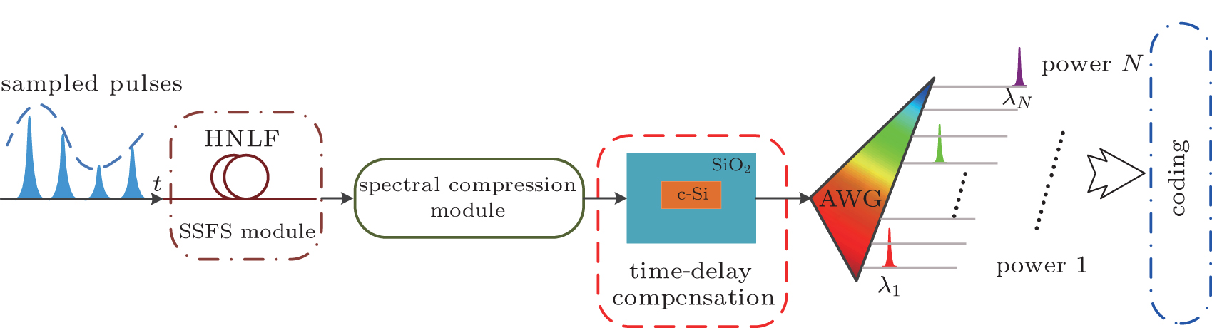
λFWHM should be achieved. In the present paper, the strip silicon waveguide is utilized to realize time-delay compensation after SSFS instead of DCF or PCF, as well as to meet the demands of miniaturization and photonic integration, which is the development trend of all-optical ADC. Owing to the inherent limitations of length, TPA, FCA, and FCD, it is difficult for the proposed all-optical ADC to realize more than 2-bit quantization. However, it is possible to combine the proposed all-optical ADC with the spectral compression scheme to obtain a smaller Δ
λFWHM and a higher quantization resolution
N after the SSFS module as shown in Fig.
10.
5. ConclusionsIn this paper, we propose a lumped time-delay compensation scheme based on the silicon waveguide for simplifying the structure and ensuring the coding correctness of the all-optical ADC by SSFS effect. The corresponding TDLs could be replaced by a short silicon waveguide to realize time-delay compensation and integration. The simulation results show that the strip silicon waveguide can compensate for the time-delay accurately with an FWHM variation of less than 2.52 ps. The proposed scheme can support an MSSR of 50.45 GSa/s with no coding error. When a spectral compression module can be added by utilizing a span of HNLF after the SSFS module, a potential 3-bit resolution can be realized since the total wavelength range is 30 nm. The lumped time-delay compensation scheme utilizing the large dispersion strip silicon waveguide instead of the multiple TDLs and fiber reduces the structure complexity in practical applications, which conforms to the trend of integration and miniaturization of all-optical ADC.


 , Shi Zhi-Guo1, Kang Zhe2, Yu Chong-Xiu2, Wang Jian-Ping1]