


Design and fabrication of multi-channel photodetector array monolithic with arrayed waveguide grating
[Lv Qian-Qian, Pan Pan, Ye Han, Yin Dong-Dong, Wang Yu-Bing, Yang Xiao-Hong, Han Qin†,  ]
]
]
|
|


† Corresponding author. E-mail:
Project supported by the National High Technology Research and Development Program of China (Grant Nos. 2013AA031401, 2015AA016902, and 2015AA016904), the National Natural Science Foundation of China (Grant Nos. 61176053, 61274069, and 61435002), and the National Basic Research Program of China (Grant Nos. 2012CB933503 and 2013CB932904).
We have provided optical simulations of the evanescently coupled waveguide photodiodes integrated with a 13-channels AWGs. The photodiode could exhibit high internal efficiency by appropriate choice of layers geometry and refractive index. Aseamless joint structure has been designed and fabricated for integrating the output waveguides of AWGs with the evanescently coupled waveguide photodiode array. The highest simulation quantum efficiency could achieve 92% when the matching layer thickness of the PD is 120 nm and the insertion length is 2 μm. The fabricated PD with 320-nm-thick matching layer and 2-μm-length insertion matching layer present a responsivity of 0.87 A/W.
Due to the increasing demand for speed and capacity of telecommunication systems, dense wavelength-division multiplexing (DWDM) systems with 40 Gb/s channel capacity are widely deployed by major telecommunication carriers to use the existing fiber infrastructure more efficiently.[1] Photonic integrated circuit (PIC) technology optimizes the manufacturing process by choosing InP-based materials, with which it is possible to realize all of the necessary optical functions on a single semiconductor chip.[2] As a multiplexer/demultiplexer, the arrayed waveguide grating (AWG) is the key component in WDM.[3] Photodetectors integrated with AWGs 16×2.5 Gb/s[4] and 10×10 Gb/s[5] have been reported, but the coupling loss is relatively high due to the use of PIN photodiodes.
Evanescently coupled waveguide photodetectors (ECPDs) are key devices in the field of digital, as well as analogue, optical transmissions, due to their high bandwidth and high responsivity.[6–8] This structure permits the efficiency and bandwidth to be specified independently because the internal efficiency is determined not by the thickness but by the length of the photoabsorption layer.[9] The ECPDs can afford high optical coupling efficiency. At the same time, it can achieve higher saturation current than a side-illuminated approach due to more uniform light absorption.[10] Responsivity higher than 1 A/W and bandwidth of 48 GHz have been reported.[11] In addition, their major advantages are the ease of integration with other optoelectronic devices to realize complex systems.[12]
As the epitaxial structure of the evanescently coupled waveguide photodetector[13] and AWGs is quite different, the monolithic configuration has been a design consideration. This letter reports the design concept and numerical simulation results of evanescently coupled photodiodes integrated with AWGs for high quantum efficiency. We optimize the structure of PD and AWGs by choosing appropriate layers’ geometry and refractive index. Monolithic integration of photodetector array and AWGs is demonstrated and the device’s performance is investigated.
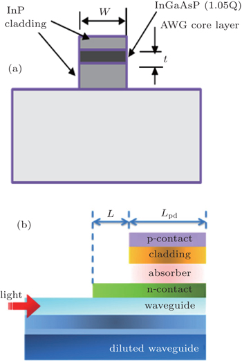
The cross section of the AWGs output waveguide is shown in Fig.
 | Fig. 1. (a) Cross section of the AWG output waveguide; (b) the lateral section of the ECPD. |
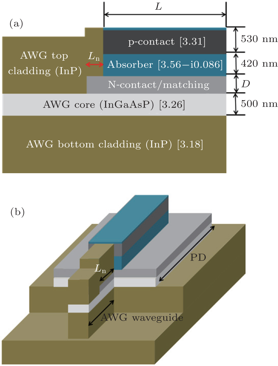 | Fig. 2. (a) Cross section of the integrated structure; (b) the schematic structure of the ECPD integrated with the AWG output waveguide. |
We design a PD array integrated with 13 output channels of AWGs in a seamless joint structure between the AWG output waveguide and the photodiode, a simple schematic structure as shown in Fig.
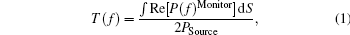
Simulations of the structure are carried out using 3D finite-difference time-domain (FDTD) solutions. In the FDTD solutions, the optical transmissivity is defined as
We suppose the light in the output waveguide of AWGs is a stable single-mode, so the mode source is used and set in the waveguide 10 μm apart from the photodiode. The length of the photodiode is fixed to 40 μm, and the width of the photodiode is fixed to 5 μm. To reach a high bandwidth, we define a 0.42-μm-thick absorption layer. For the optimization of the optical structure, three important parameters are identified: the thickness and refractive index of InGaAsP (λg < 1.33 μm) matching layer above the core layer, the length (Ln) of the matching layer inserted into the AWGs top cladding layer.
The optical matching layer, which also serves as the n-contact layer, provides a refractivity match between the waveguide and the absorption layer to reduce the reflection loss of the refractivity saltation. Therefore, the refractive index affects the optical intensity distribution in the p–i–n photodiode. For a given thickness of the matching layer, we find that light can be rapidly coupled into the absorber with high refractive index of the matching layer as shown in Fig.
Figure
 | Fig. 3. Absorption efficiency as a function of the device length L with different matching layer refractive indexes. |
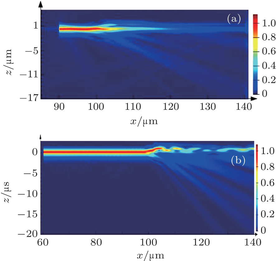 | Fig. 4. (a) Longitudinal section of the electric field distribution in device without absorption coefficient when the refractive index of matching layer is 3.255; (b) the longitudinal section of the electric field distribution in device without absorption coefficient when the refractive index of matching layer is 3.41. |
The thickness is another factor to beating effect. For the seamless structure, changing the matching-layer thickness, then the optimized matching layer thickness will be determined and the simulated result is shown in Fig.
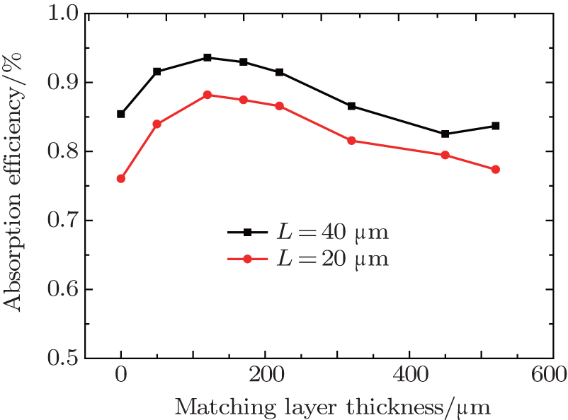 | Fig. 5. Absorption efficiency as a function of matching layer thickness D with different device length L. |
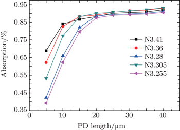
At the interface, in order to enhance the coupling efficiency, a portion of matching layer with length of Ln is inserted into the AWG cladding layer. The Ln influences the electric field distribution at the absorber interface due to the beating effect. The influence of the matching layer insertion length Ln and the optical characteristic of this structure is studied. The typical simulation results of the absorption efficiency versus the matching layer insertion length Ln are presented in Fig.
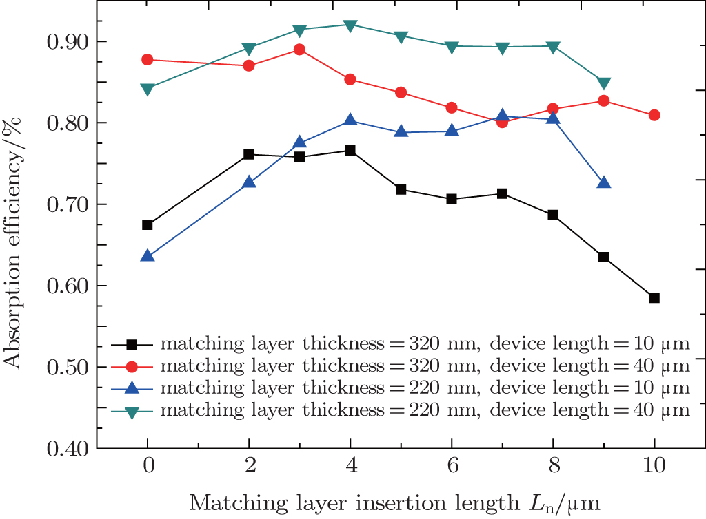 | Fig. 6. Absorption efficiency as a function of insertion length Ln with different device length L and matching layer thickness D. |
After obtaining these simulation results, the epitaxial structure with optimized parameters was grown using the metalorganic chemical vapour deposition (MOCVD) technique on an InP semi-insulating substrate. For the seamless structure, the first epitaxial structure consists of an AWG bottom cladding layer, core layer, and the p–i–n structure as shown in Table
| Table 1. The first epitaxial structure of the integrated device. . |
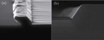
The results of the regrowth epitaxial structure are shown in Fig.
 | Fig. 7. The scanning electron micrograph (SEM) images of the regrowth structure: (a) the epitaxial structure by SAG in [011] orientation; (b) the epitaxial structure by SAG in [0 −1 1] orientation. |
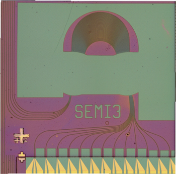
Device fabrication is carried out using conventional lithography techniques and standard InP processing techniques. Firstly, the p mesa was etched down to the n-contact layer with a sequence of wet etching and inductively coupled plasma (ICP) etching. Secondly, the larger n mesa was etched down into the un-doped waveguide layer. Thirdly, the device was passivated and the contact metals deposited. Finally, an SiO2 layer was grown by plasma enhanced chemical vapor deposition (PECVD) as a hard mask and AWGs structure was formed by a lithography step and inductively coupled plasma (ICP) etching.
 | Fig. 8. Microscopeimage of the fabricated ECPD array integrated with a 13-channel AWG. |
 | Fig. 9. The measured current as a function of the bias voltage with seamless structure. |
Figure
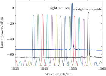
 | Fig. 10. The spectral response of the fabricated AWG without regrowth. |
In this letter, we have designed and optimized the epitaxial structures of evanescently coupled photodiodes integrated with AWGs. A higher absorption efficiency of 85% is achieved by seamless joint between the AWG and PDs, in which the thickness of matching layer is 320 nm and the insertion length is 2 μm. The experiment result is 0.87 A/W, which is consistent with the simulation results. According to the theoretical calculation, the individual devices could realize a bandwidth more than 10 GHz, which are integrated with a 10-channels AWGs and can reach a high capacity of 100 Gb/s.
| 1 | |
| 2 | |
| 3 | |
| 4 | |
| 5 | |
| 6 | |
| 7 | |
| 8 | |
| 9 | |
| 10 | |
| 11 | |
| 12 | |
| 13 |