Li Liuan, Zhang Jiaqi, Liu Yang, Ao Jin-Ping. Evaluation of a gate-first process for AlGaN/GaN metal-oxide-semiconductor heterostructure field-effect transistors with low ohmic annealing temperature. Chinese Physics B, 2016, 25(3): 038503
Permissions
Evaluation of a gate-first process for AlGaN/GaN metal-oxide-semiconductor heterostructure field-effect transistors with low ohmic annealing temperature
Li Liuan1, Zhang Jiaqi2, Liu Yang1, †, , Ao Jin-Ping2, ‡,
School of Microelectronics, Sun Yat-Sen University, Guangzhou 510275, China
Institute of Technology and Science, Tokushima University, Tokushima 770-8506, Japan
Project supported by the International Science and Technology Collaboration Program of China (Grant No. 2012DFG52260).
Abstract
Abstract
In this paper, TiN/AlOx gated AlGaN/GaN metal–oxide–semiconductor heterostructure field-effect transistors (MOS-HFETs) were fabricated for gate-first process evaluation. By employing a low temperature ohmic process, ohmic contact can be obtained by annealing at 600 °C with the contact resistance approximately 1.6 Ω·mm. The ohmic annealing process also acts as a post-deposition annealing on the oxide film, resulting in good device performance. Those results demonstrated that the TiN/AlOx gated MOS-HFETs with low temperature ohmic process can be applied for self-aligned gate AlGaN/GaN MOS-HFETs.
Self-aligned gate (SAG) structure is an effective method for minimizing the access region (access resistance) of AlGaN/GaN HFETs, which is critical to develop a high-power and high-frequency device.[1,2] The SAG structure requires that the Schottky gate can withstand the ohmic annealing temperature because the gate and ohmic electrodes are annealed simultaneously.[3] The widely used Ti/Al-based multilayers on AlGaN/GaN HFETs need a high temperature (commonly above 700 °C) to form ohmic contact, which usually causes serious gate electrode degradation. Therefore, a thermal stable gate material and/or a low temperature ohmic process are beneficial for the SAG structure.
The TiN electrode with good thermal stability is a prospective gate candidate for a self-aligned gate process. The TiN-gated transistor showed the lowest ohmic contact resistance and the highest maximum drain current annealing at 800 °C for 1 min. However, the gate leakage current increased after high temperature ohmic annealing.[4] MOS-HFETs with TiN/AlOx stack gate layer were proposed to decrease the gate leakage current.[5] However, the formation of microcrystalline structures after annealing at 700 °C causes the loss of the dielectric function.[6] Furthermore, the exploration of dielectric with a high crystalline temperature (above 800 °C) is difficult. Therefore, a low temperature ohmic process is very necessary.
Recently, with the assisting of inductivity coupled plasma (ICP) treatment, ohmic metal of Ti/Al/Ti/Au can realize good ohmic contact on n+-GaN without annealing.[7] The ICP treatment can introduce etching damage and form an n+-GaN layer owing to the formation of nitrogen vacancy, which can help to get a low ohmic annealing temperature. Herein, by using a low temperature ohmic process (at 600 °C), TiN/AlOx gated MOS HFETs were fabricated for the gate-first process evaluation. The results show that this process is beneficial for the fabrication of self-aligned gate AlGaN/GaN MOS-HFETs.
2. Device fabrication
The epitaxial wafer of the AlGaN/GaN HFETs was grown on silicon substrate by metal organic chemical vapor deposition. The wafer structure consisted of a nucleation layer (approximately 30 nm thick), a 300-nm buffer layer, a 1-μm undoped GaN channel layer, a 25-nm unintentionally doped Al0.25Ga0.75N barrier layer, and a GaN cap layer of about 2 nm from the bottom to the top. The average sheet resistance of the two-dimensional electron gas obtained from Hall measurement at room temperature is about 385 Ω/◻.
As shown in Fig. 1, the device fabrication process began with mesa isolation, which was formed by a Cl2/SiCl4 plasma etching through ICP with an etching depth of 60 nm. As an evaluation method for the gate-first process, we deposited the ohmic and gate electrodes in-order and then annealed together. Before the deposition of ohmic metal, the surface was treated using SiCl4 plasma (20 s at 0.25 Pa) with an ICP power and bias of 100 W and 100 W, respectively, in an ICP system. The treated samples were immersed into the BHF/HNO3 (1:1) for 30 s. Then, ohmic metal was formed using an Al/Ti/Au (200/40/40 nm) multi-layer structure. The AlOx layer (approximately 20 nm) and TiN gate film (approximately 100 nm) were deposited using reactive sputtering in different ambient environment with metal targets.[4,5] Finally, the samples were annealed at 600 °C for 1 min to obtain ohmic contact. The electrical properties of the devices were evaluated systematically.
3. Characteristics and discussion
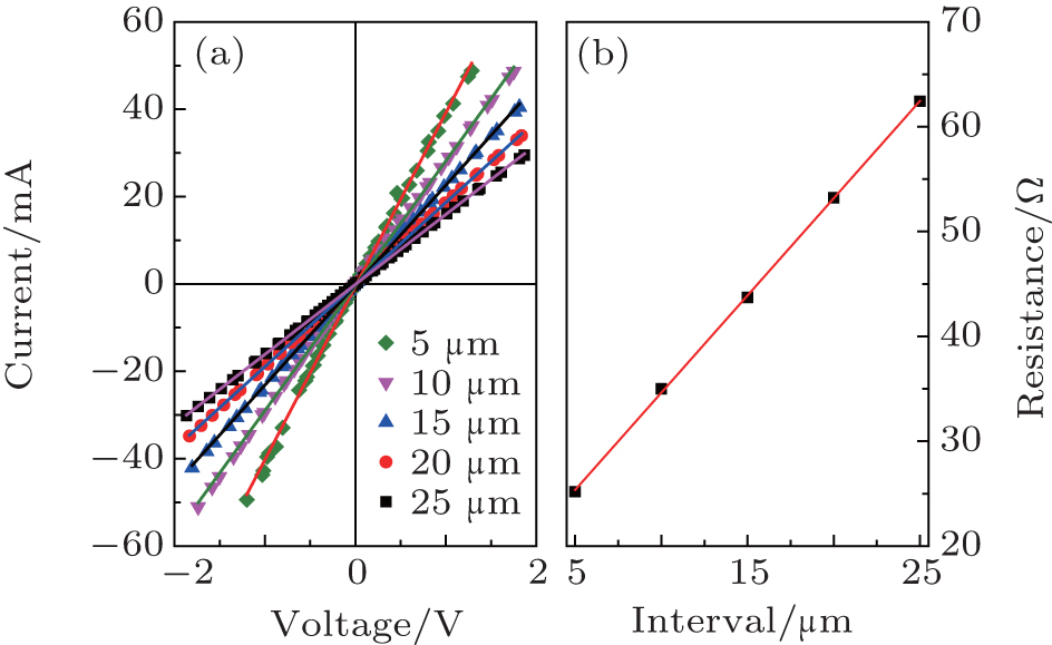
The ohmic contact was evaluated by transmission line model (TLM) method. Figure 2(a) shows the current–voltage (I–V) characteristics recorded on the TLM patterns with an interval of 5, 10, 15, 20, and 25 μm, respectively, and a width of 200 μm. The linear curves suggest that the good ohmic contact behavior was formed between the metal stack and the semiconductor. An ohmic contact resistance of 1.6 Ω·mm (6.97× 10⁻⁵ Ω·cm2) and a sheet resistance of 371 Ω/◻ were obtained from the plot of the corresponding resistance versus the interval (Fig. 2(b)). The ICP treatment is reported to produce a damage layer (mainly nitrogen vacancies) on the surface of AlGaN as well as to decrease the thickness of the AlGaN layer. Therefore, the enhanced tunneling current will dominate the current, forming a good ohmic contact even when annealed at a low temperature of 600 °C.[7]
Fig. 2. The current–voltage (a) and TLM characteristics (b) of the ohmic contact.
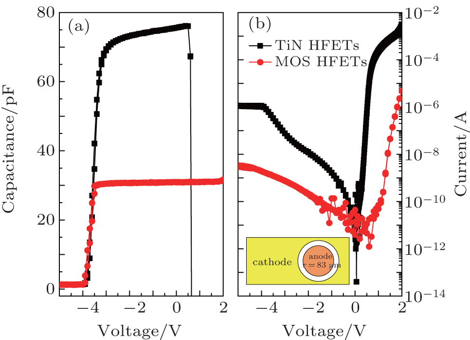
Figure 3(a) shows the high frequency (1 MHz) capacitance–voltage (C–V) measurements of the MOS and the reference HFETs. The measurements were performed on a circular diode structure with a diameter of 166 μm (inset in Fig. 3(b)). As expected, the presence of AlOx dielectric in the MOS HFETs caused a decrease of the accumulation capacitance with respect to the reference one. The sharp transition as well as the negligible hysteresis in the curve of TiN-gate reference HFETs demonstrates a low interfacial state density at the heterojunction. For the MOS-HFETs, the ohmic annealing at about 600 °C also can act as the post-deposition annealing for the dielectric film. The post-deposition annealing can decrease the interfacial state density and improve the trapping behavior, resulting in a slightly stretched curve with no obvious hysteresis.[5] If the sheet charge density in the channel at zero gate bias is the same for both devices and assumung that there is no surface charge at the dielectric/AlGaN interface, the MOS-HFETs should exhibit a negative threshold voltage (Vth) shift to approximately −9 V theoretically.[8] However, the Vth determined from linear fitting of the high slope regions of the curves are comparable for HFETs and MOS-HFETs. As discussed in our previous report, the thermal treatments can eliminate the positive charge accumulation in the oxide and generate negatively charged traps and interface states or negative fixed/mobile charges, leading to the positive Vth shift.[5] The origin of the negative charges at the interface or in the AlOx layer is not clear now. However, it was reported that oxygen atoms from the AlOx layer reacted with Ga atoms to form a GaOxNy oxygen-rich interfacial layer, which was responsible for an increase in negative charge.[9] Besides this, interstitial oxygen was also reported to cause the presence of negative charges.[10] Therefore, a possible origin of the negative charges is the oxygen bonding state variation during the post-deposition annealing process.
Fig. 3. The capacitance–voltage (a) and current–voltage (b) characteristics of MOS-HFETs.
The logarithmic plot of the I–V characteristics for circular HFETs and MOS-HFETs was shown in Fig. 3(b). The TiN-gated HFETs show good rectifying characteristics with a reverse leakage current of 10−6 A. It is found that the reverse leakage current rises as the external bias increases and finally saturates at approximately −4 V. Further increasing the reverse bias leads to very small increase of the magnitude of the leakage current. The saturation behavior of the reverse leakage current is associated with full depletion of the 2DEG at the AlGaN/GaN interface.[11] As can be seen, the introduction of an AlOx layer as gate insulator leads to a reduction of the reverse leakage current (to approximately 10−9 A). The leakage current transport mechanism in the MOS-HFETs was ascribed to the Frenkel–Poole emission in our previous report.[5]
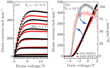
Figure 4(a) shows the I–V characteristics of the bar-type reference HFETs and the MOS-HFETs. The gate length and the gate-source/drain spacing of the bar-type devices are 3 and 3 μm, respectively. Both of the devices present good pinch-off characteristics and operation up to gate voltage of 2 V was confirmed. It is seen that the drain current is approximately 500 mA/mm for the reference HFETs and is approximately 450 mA/mm for the MOS-HFETs. The relatively smaller maximum drain current and gm compared with the reference device (Fig. 4(b)) is attributed to a larger separation between the gate and the 2DEG channel with the presence of AlOx. The average mobility and sheet charge density of the two-dimensional electron gas can also be calculated from the FAT-FETs (gate length is 100 μm) of approximately 2025 cm2·V−1·s−1 and 8.32×1012 cm2, respectively.
Fig. 4. The current–voltage (a) and transfer (b) characteristics of HFETs and MOS-HFETs.
The interface state information can be obtained from the subthreshold swing of the bar-type devices. As calculated from Fig. 5, the corresponding subthreshold swing of the HFETs is around 106.22 mV/decade, while it is approximately 96.86 mV/decade for the MOS-HFETs. The lower subthreshold swing value can be attributed to the reduced interfacial state density and the improved trapping behavior of the dielectric inside the oxide and/or at the interface. The off-state drain leakage current of the bar-type HFETs and MOS HFETs are comparable because the leakage current along the isolation region dominates the leakage current.
Fig. 5. The subthreshold swing characteristics of bar-type devices.
4. Conclusion
A low temperature ohmic annealing process was used to fabricate MOS-HFETs with an AlOx dielectric. With the assistance of ICP treatment, ohmic contact can be obtained at 600 °C with a resistance of approximately 1.6 Ω·mm. The MOS-HFETs fabricated with such a process possess a smaller hysteresis and reverse gate leakage current after the ohmic annealing process. The introduction of this low temperature ohmic is beneficial for the fabrication of self-aligned gate AlGaN/GaN MOS-HFETs with an AlOx layer.
Evaluation of a gate-first process for AlGaN/GaN metal-oxide-semiconductor heterostructure field-effect transistors with low ohmic annealing temperature
[Li Liuan1, Zhang Jiaqi2, Liu Yang1, †, , Ao Jin-Ping2, ‡, ]


 , Ao Jin-Ping2, ‡,