
Two-dimensional models of threshold voltage and subthreshold current for symmetrical double-material double-gate strained Si MOSFETs
[Xin Yan-hui1, 2, Yuan Sheng1, Liu Ming-tang1, Liu Hong-xia2, †,  , Yuan He-cai3]
, Yuan He-cai3]
 |


† Corresponding author. E-mail:
Project supported by the National Natural Science Foundation of China (Grant Nos. 61376099, 11235008, and 61205003).
The two-dimensional models for symmetrical double-material double-gate (DM-DG) strained Si (s-Si) metal–oxide semiconductor field effect transistors (MOSFETs) are presented. The surface potential and the surface electric field expressions have been obtained by solving Poisson’s equation. The models of threshold voltage and subthreshold current are obtained based on the surface potential expression. The surface potential and the surface electric field are compared with those of single-material double-gate (SM-DG) MOSFETs. The effects of different device parameters on the threshold voltage and the subthreshold current are demonstrated. The analytical models give deep insight into the device parameters design. The analytical results obtained from the proposed models show good matching with the simulation results using DESSIS.
As metal oxide semiconductor devices have been scaled down continuously, the channel length has been shortened, and how to suppress the short channel effects (SCEs), the drain induced barrier lowering (DIBL) effect and increasing the carrier transport efficiency becomes an attractive problem.[1–3] It becomes obligatory to find out the solution of this problem to improve the device performance. Many reports show that the mobility of the charge carriers can be enhanced through the strain technology.[4,5] A strain can result in an enhanced mobility, a modified lattice constant of the material, and an energy band structure to trap carriers. Thus, strained Si (s-Si) metal–oxide semiconductor field effect transistors (MOSFETs) have received a great deal of attention.[6] However, the higher degree of impact ionization leads to the higher density of interface traps which in turn degrades both DIBL and SCEs.[7]
Double-gate (DG) and multi-material gate MOSFET structures can suppress the SCEs and DIBL in an excellent way. Many theoretical and experimental studies have reported that the DG device has excellent short-channel effect immunity, an ideal subthreshold factor, and high transconductance.[8–10] Multi-material gate MOSFET structures, like double-material gate (DMG) MOSFETs, are proposed to suppress SCEs. These structures have two or three metals in the gate with different work functions.[11] Long et al. first proposed the DMG MOSFET structure,[12] and demonstrated that the novel structure can increase the carrier transportation efficiency and suppress SCEs. The DMG structure can improve the device performance.
In light of these facts, for the first time, we present the two-dimensional models of threshold voltage and subthreshold current for symmetrical DM-DG s-Si MOSFET by incorporating the double-material double-gate concept into the bi-axially strained channel device. By solving Poisson’s equation, the surface potential can be obtained. The proposed models are derived based on the surface potential. In the channel region, Poisson’s equation is solved by the parabolic approximation method with suitable boundary conditions.[13] The effects of various device parameters on the threshold voltage and the subthreshold current are demonstrated. Different length ratios are optimized to minimize the SCEs and the leakage current of the device. The derived analytical models give results that agree well with those of the 2D device simulator DESSIS.
The device structure is shown in Fig.
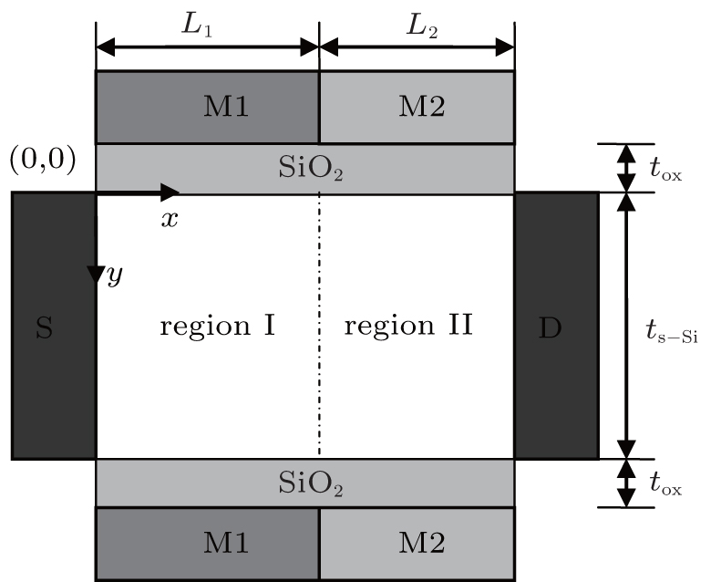 | Fig. 1. Schematic diagram of symmetrical DM-DG s-Si MOSFET. |
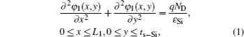
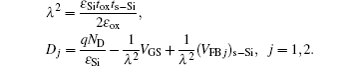
The whole potential distribution is divided into the two regions in the s-Si layer. The potentials φ1 and φ2 belong to region I and region II, respectively. The x axis and the y axis are parallel and perpendicular to the channel, respectively. Poisson’s equation in the two regions can be written as[13]

The potential of the s-Si layer in the vertical direction can be approximated as[13]

By applying Eq. (


Equation (


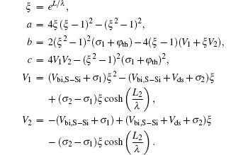
The control gate region which has the higher work function mainly monitors the threshold voltage of the device. So the threshold voltage is determined by φS1 min.
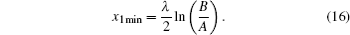
By solving dφS1(x)/dx = 0 defined in Eq. (

The electric field pattern along the channel determines the electron transport velocity. The surface electric fields in region I and region II are given respectively by


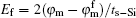
The conventional definition of threshold voltage of MOSFETs is the gate source voltage at which φSmin = 2φF,Si, where φF,Si is the difference between the extrinsic Fermi level in the bulk region and the intrinsic Fermi level.[14] By considering the effect of strain, the threshold condition of the front gate for the present symmetrical DM-DG s-Si MOSFET is modified as[14,15]


The diffusion phenomenon mainly determines the subthreshold current which is proportional to the carrier concentration at the position of the minimum channel potential. By applying the methodology used in Ref. [16], the subthreshold current can be expressed as


In this paper, the analytical results obtained from the derived models are compared with the numerical simulation results using DESSIS. The doping concentration of the source–drain contact regions is NDS = 1 × 1020 cm−3. The device is simulated by using the drift-diffusion model for the carrier transport and the field-dependent mobility model because of the high electric fields in the device.
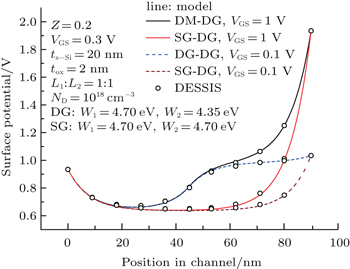
Figure
 | Fig. 2. Surface potentials in DM-DG and SM-DG MOSFETs with various drain voltages. |
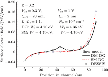
Figure
 | Fig. 3. Surface electric fields in DM-DG and SM-DG s-Si MOSFETs. |
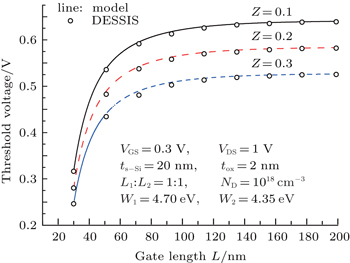
Figure
 | Fig. 4. Threshold voltages with different strains. |
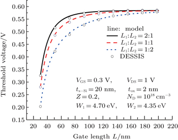
Figure
 | Fig. 5. Threshold voltages with different gate length ratios. |
Figure
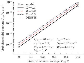
 | Fig. 6. Variation of subthreshold current with strain. |
Figure
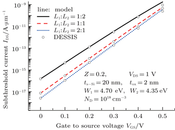
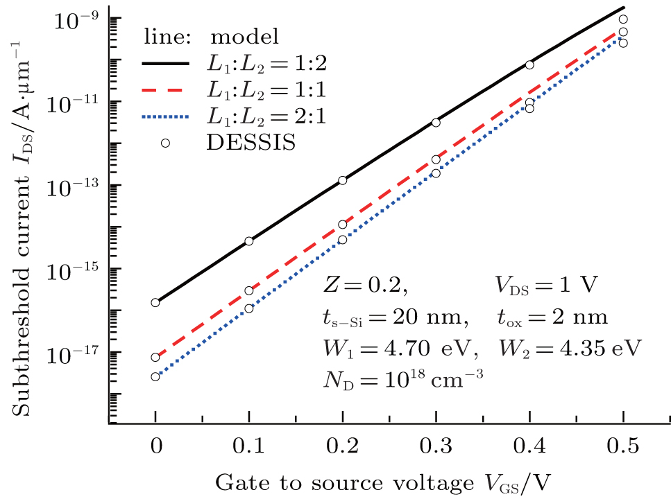 | Fig. 7. Variation of subthreshold current with gate length ratio. |
The two-dimensional models of threshold voltage and subthreshold current for symmetrical double-material double-gate strained Si MOSFETs have been presented. The surface potential has been obtained for a different drain voltage. A detailed analysis of the impact of various device parameters on the threshold voltage and the subthreshold current has been given. It is demonstrated that the threshold voltage decreases and the subthreshold current increases with increasing strain. The leakage current and SCEs can be controlled desirably by increasing the gate length ratio. The analytical models give accurate results as compared to the simulations. The analytical models give valuable references to the physical parameter design.
| 1 | |
| 2 | |
| 3 | |
| 4 | |
| 5 | |
| 6 | |
| 7 | |
| 8 | |
| 9 | |
| 10 | |
| 11 | |
| 12 | |
| 13 | |
| 14 | |
| 15 | |
| 16 | |
| 17 |