


Effect of lateral structure parameters of SiGe HBTs on synthesized active inductors
[Zhao Yan-Xiao, Zhang Wan-Rong†,  , Xin Huang, Xie Hong-Yun, Jin Dong-Yue, Fu Qiang]
, Xin Huang, Xie Hong-Yun, Jin Dong-Yue, Fu Qiang]


† Corresponding author. E-mail:
Project supported by the Natural Science Foundation of Beijing, China (Grant Nos. 4142007 and 4122014), the National Natural Science Foundation of China (Grant No. 61574010), and the Higher Educational Science and Technology Program of Shandong Province, China (Grant No. J13LN09).
The effect of lateral structure parameters of transistors including emitter width, emitter length, and emitter stripe number on the performance parameters of the active inductor (AI), such as the effective inductance Ls, quality factor Q, and self-resonant frequency ω0 is analyzed based on 0.35-μm SiGe BiCMOS process. The simulation results show that for AI operated under fixed current density JC, the HBT lateral structure parameters have significant effect on Ls but little influence on Q and ω0, and the larger Ls can be realized by the narrow, short emitter stripe and few emitter stripes of SiGe HBTs. On the other hand, for AI with fixed HBT size, smaller JC is beneficial for AI to obtain larger Ls, but with a cost of smaller Q and ω0. In addition, under the fixed collector current IC, the larger the size of HBT is, the larger Ls becomes, but the smaller Q and ω0 become. The obtained results provide a reference for selecting geometry of transistors and operational condition in the design of active inductors.
Active inductors (AIs) synthesized by transistors have attracted increasing interest due to a number of unique advantages over its spiral counterpart including small chip area consumption, large inductance with wide tuning range, large and tunable quality factor, and high self-resonant frequency.[1–5] The popular synthesis method of AI is based on Gyrator-C principle. A gyrator consists of two back-to-back connected transistors as transconductors, and input capacitance Cπ of one transconductor acts as the load of the other transconductor,[1,6] then the gyrator-C behaves as a single-ended inductor. Therefore, the performance of transistors has a decisive effect on the performance of active inductor. Furthermore, the performance of transistors is almost determined by vertical and lateral structure parameters. For the transistors with the fixed vertical structure, their performance parameters are fundamentally determined by lateral structure.[7,8] Therefore, for an AI designer who relies on the library of foundry, it is important to know how to select transistors in the foundry library so as to meet the requirement of AI parameters, such as inductance Ls, quality factor Q, and self-resonant frequency ω0.
Up to now, there are many papers on synthesis of AI. It is shown that the AI parameters depend on the model parameters of transistors, such as capacitance, transconductance and resistance. Kia et al.[1,6,9] proposed novel AIs and derived that Ls can be expressed by transistor model parameters, so can Q and ω0. Kumari et al.[3] studied the dependence of Ls on the load capacitance C. Robert et al.[10] discussed the Q enhancement with the feedback resistance Rf. Chun et al.[11] discussed the effect of the input signal voltage on Ls and improved the AI linearity. However, there has been no report on the effect of lateral parameters of transistors on performance parameters of AI.
In this paper, based on library of 0.35-μm SiGe BiCMOS process, the effect of lateral parameters of transistor such as emitter width, emitter length, and emitter stripe number on performance parameters of AI is investigated. The paper is arranged as follows. In Section 2, taking a typical active inductor topology for example, the dependence of the AI parameters including the Ls, Q, and ω0 on transistor model parameters input capacitance Cπ, transconductance gm, and input resistance rπ is given. Furthermore, in Section 3, by analyzing the dependence of the transistor model parameters on HBTs lateral parameters, we obtain the analytical expressions that reveal the effect of transistor lateral parameters on the AI parameters Ls, Q, and ω0. In Section 4, based on library of 0.35-μm SiGe BiCMOS process, the effect of lateral parameters of transistors such as emitter width, emitter length, and emitter stripe number on AI parameters is verified. Finally, the conclusion is given in Section 5.
A typical SiGe HBT active inductor consists of common emitter configuration of transistor Q1 with a negative transconductance and common collector configuration of transistor Q2 with a positive transconductance, as shown in Fig.
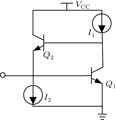 | Fig. 1. A typical SiGe HBT active inductor. |
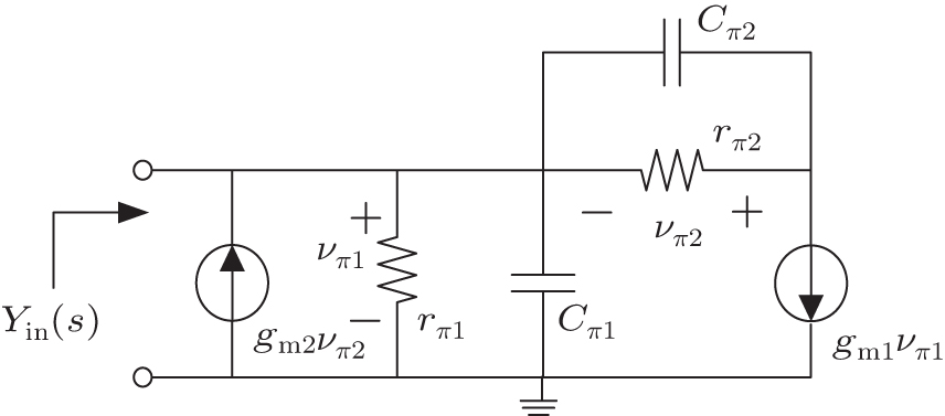 | Fig. 2. Small signal equivalent circuit. |
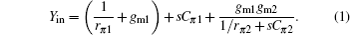
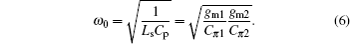
The expression (


The self-resonant frequency ω0 of RLC network of the active inductor is derived from Eqs. (
The input impedance Zin = 1/Yin has a zero at frequency

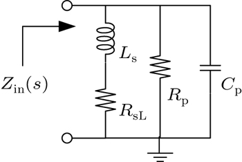
It is evident that the RLC network in Fig.
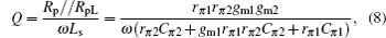
The quality factor Q of the active inductor can be expressed as
 | Fig. 3. RLC equivalent circuit. |
As shown in Section 2, the active inductor parameters Ls, Q, and ω0 depend on transistor model parameters Cπ, gm, and rπ. Obviously, they depend on the lateral structure parameters of the transistors. Therefore, the effect of the lateral structure parameters of SiGe HBTs on the AI is obtained by analyzing the dependence of Cπ, gm, and rπ on lateral structure parameters.
In general, the input resistance rπ of the transistor is expressed as

The transconductance gm of the transistor can be expressed as

The input capacitance Cπ is composed of a bottom capacitance (CBottom) and a sidewall capacitance (CSW), and Cπ can be simply described as


For simplification, the transistors Q1 and Q2 in Fig.

As shown in Eq. (
Quality factor Q is derived by substituting Eqs. (

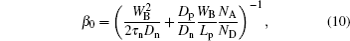
Because β0 ≫ 1, (2/β0 + 1) ≈1, equation (
Equation (
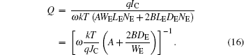
The quality factor Q is also expressed as follows:
Therefore, ω0 can be given by

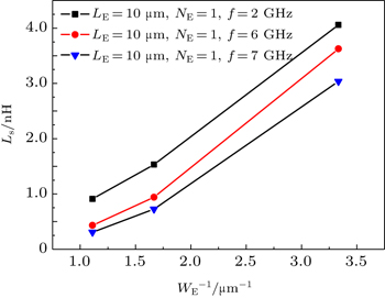
Figure
 | Fig. 4. Ls versus 1/WE at JC = 0.05 mA/μm2. |
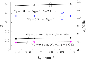
Figure
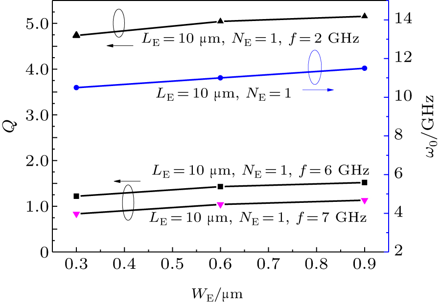 | Fig. 5. Q and ω0 versus WE at JC = 0.05 mA/μm2. |
Figure
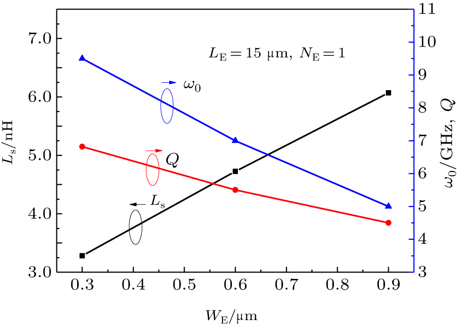 | Fig. 6. Ls, Q, and ω0 versus WE at IC = 0.2 mA. |
Figure
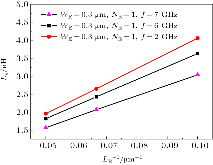 | Fig. 7. Ls versus 1/LE at JC = 0.05 mA/μm2. |
Figure
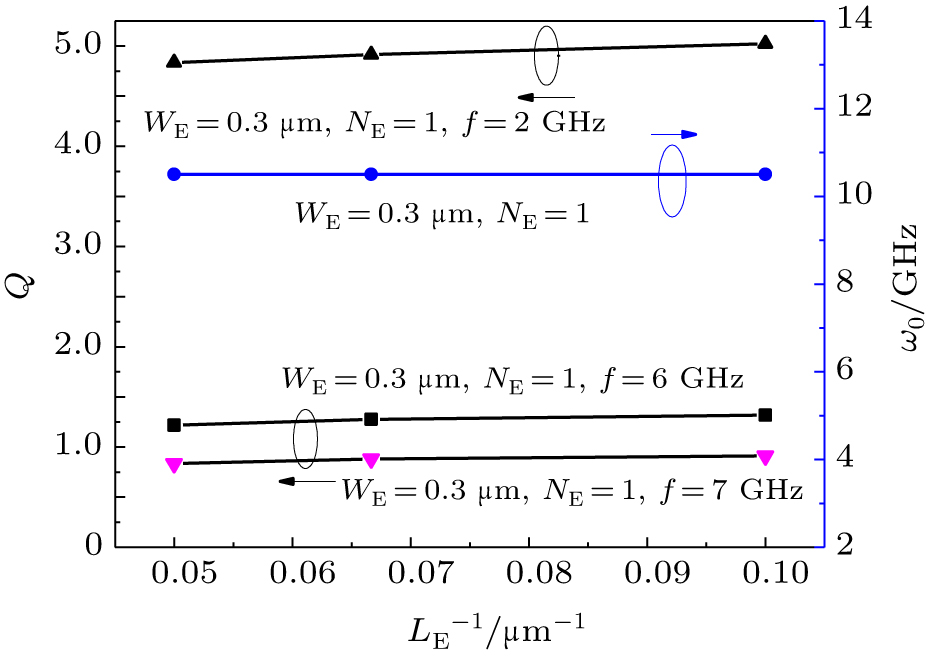 | Fig. 8. Q and ω0 versus 1/LE at JC = 0.05 mA/μm2. |
Figure
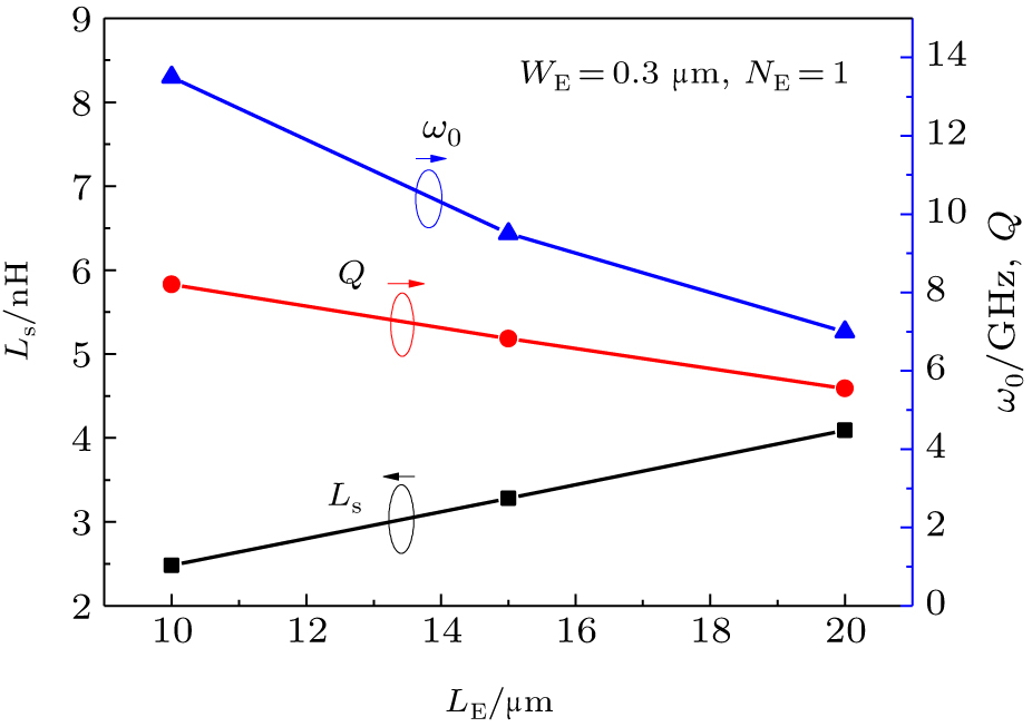 | Fig. 9. Ls, Q, and ω0 versus LE at IC = 0.2 mA. |
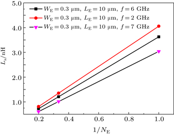
Figure
Figure
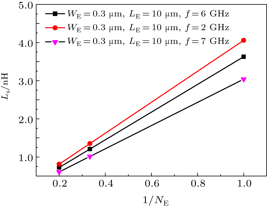 | Fig. 10. Ls versus 1/LE at JC = 0.05 mA/μm2. |
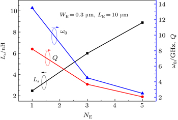
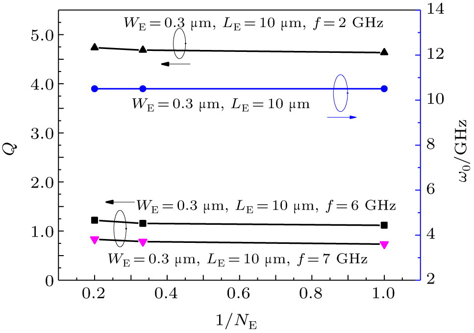 | Fig. 11. Q and ω0 versus 1/NE at JC = 0.05 mA/μm2. |
Figure
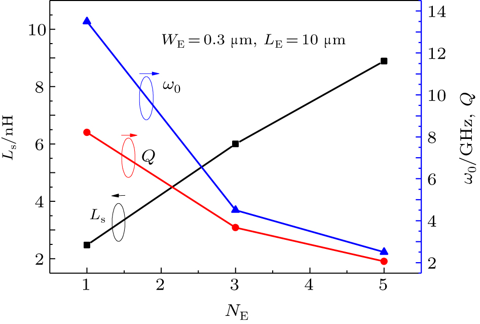 | Fig. 12. Ls, Q, and ω0 versus WE at IC = 0.2 mA. |
The above results are obtained at the fixed collect current density and the fixed collect current, respectively. Figure
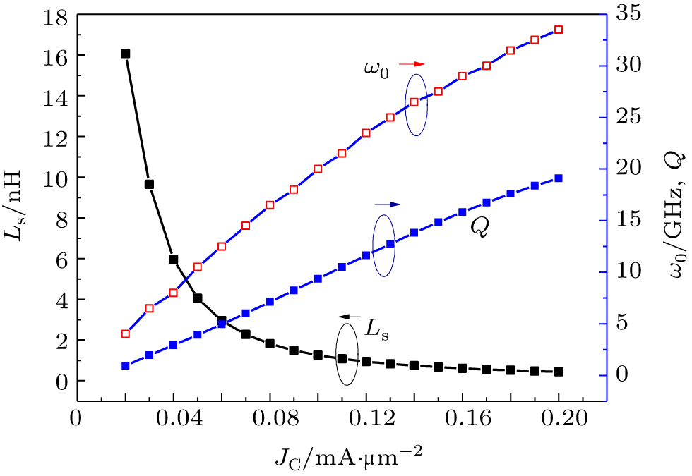 | Fig. 13. Ls, Q, and ω0 versus the collect current density JC at a fixed size of HBTs. |
In the paper, we analyze the effect of lateral structure parameters including emitter width, length and emitter stripe number of HBT on the performance parameters of the active inductor (AI), such as inductance Ls, quality factor Q, and self-resonant frequency ω0 based on library of 0.35-μm SiGe BiCMOS process. The simulation results show that for a given collector current density JC, the large Ls of the AI can be obtained by the narrow, short emitter stripe and few emitter stripes, but Q and ω0 have little dependence on the geometry sizes of SiGe HBTs. For a fixed HBT size, smaller JC is beneficial for AI to obtain larger Ls, but with a cost of smaller Q and ω0. In addition, for the fixed collector current IC, the large HBT size results in large Ls, but small Q and ω0. Therefore, in the design of an AI, a tradeoff exists among the AI parameters, the lateral structure parameters of HBT, and operational current density or operational current. The obtained results provide a basis for selecting the transistors lateral geometry from the library of foundry and operational condition in the design of active inductors.
| 1 | |
| 2 | |
| 3 | |
| 4 | |
| 5 | |
| 6 | |
| 7 | |
| 8 | |
| 9 | |
| 10 | |
| 11 | |
| 12 |