


Design of a multiband terahertz perfect absorber
[Hu Dan1, †,  , Wang Hong-yan2, Tang Zhen-jie1, Zhang Xi-wei1, Ju Lin1, Wang Hua-ying3, ‡, ]
, Wang Hong-yan2, Tang Zhen-jie1, Zhang Xi-wei1, Ju Lin1, Wang Hua-ying3, ‡, ]
|
|


† Corresponding author. E-mail:
‡ Corresponding author. E-mail:
Project supported by the National Natural Science Foundation of China (Grant No. 11504006), the Key Scientific Research Project of Higher Education of Henan Province, China (Grant No. 15A140002), and the Science and Technology Planning Project of Henan Province, China (Grant No. 142300410366).
A thin-flexible multiband terahertz metamaterial absorber (MA) has been investigated. Each unit cell of the MA consists of a simple metal structure, which includes the top metal resonator ring and the bottom metallic ground plane, separated by a thin-flexible dielectric spacer. Finite-difference time domain simulation indicates that this MA can achieve over 99% absorption at frequencies of 1.50 THz, 3.33 THz, and 5.40 THz by properly assembling the sandwiched structure. However, because of its asymmetric structure, the MA is polarization-sensitive and can tune the absorptivity of the second absorption peak by changing the incident polarization angle. The effect of the error of the structural parameters on the absorption efficiency is also carefully analyzed in detail to guide the fabrication. Moreover, the proposed MA exhibits high refractive-index sensing sensitivity, which has potential applications in multi-wavelength sensing in the terahertz region.
Metamaterials, artificial electromagnetic media that are structured on the subwavelength scale, have received considerable attention due to their exotic physical properties that are normally unavailable in nature, such as the negative index of refraction,[1] the inverse Doppler effect,[2] and so on. By using these artificial metamaterials with extraordinary properties, researchers can make invisibility cloaks,[3] perfect lenses,[4] absorbers[5,6] or other devices.[7] The metamaterial-based absorber is an important application of metamaterials. Through designing the physical scale of the structure and orderly arranging it, researchers can develop a metamaterial absorber (MA) with many excellent properties, for example a thin product which is not limited to one-quarter wavelength thickness, and which has high absorption, and is small-sized, etc. The first perfect MA, having the experimental absorptivity of about 88% at microwave frequencies, composed of an electrical ring resonator and a split wire separated by a dielectric layer, was demonstrated by Landy et al.[8] Since then, the perfect absorbers have attracted considerable interest, and a large number of absorbers have been proposed and demonstrated from microwave to optical frequencies.[9–12]
As a matter of fact, the development of the perfect MA is especially attractive at terahertz (THz) frequencies where it is not easy to find naturally occurring materials with strong absorption coefficients. Such absorbers could clearly be of use for thermal imaging, thermal bolometry, wavelength selective radiation, stealth technology, and nondestructive detection. A lot of effort has been made to achieve THz metamaterial absorbers with perfect absorption. Tao et al. obtained an absorptivity of 97% at 1.6 THz;[13] Landy et al. and Grant et al. gained a polarization-insensitive MA, respectively.[14,15] However, all these efforts shared the common shortcoming of single band absorption, which becomes an obstacle to their practical applications. However, in many cases, such as THz spectroscopic imagers and detectors, an absorber with multiband is required, since the detector based on the multiband absorber can realize frequency selective detection, decrease the environmental disturbance, and consequently increase the detection sensitivity and imaging resolution. One of the effective methods of multiband operation is to use single-layer structure with two or multiple resonators.[16–21] Following this design strategy, multiband (or broadband) absorbers have been demonstrated in a wide frequency region ranging from microwave to optics,[22–24] but the same shape resonator will result in significant mutual coupling between several elements when the positions of several metallic patches are close to each other. An alternative method is to use multiple vertically stacked metallic layers to obtain the multiband metamaterial absorbers, each absorption band corresponding to a specific layer.[25–28] Another approach for making multiple absorber bands is to utilize single-layer dielectric structure with one metallic element constructed of a special geometric shape.[29,30] However, both of these structures are very complicated, imposing considerable restrictions on both design and fabrication. Although the metamaterial absorbers have been demonstrated effectively to make multiband absorption, the designs are mostly based on the overlapping of the fundamental resonance of the regular single-band absorber. There is little novelty in designing the new types of multiband absorbers.
In comparison to previous designs, the proposed multiband MA in this paper has several important advantages. Most importantly, it is formed by a U-shaped metallic ring and metallic ground plane, separated by a dielectric layer, so the structure is very simple and easy to fabricate. In addition, it presents three absorption peaks in the designed structure and is made on a highly thin-flexible polyimide substrate with a total thickness of 9.4 μm, which can be used in the non-planar case. Moreover, the multiband absorption peaks in our designed metamaterial structure exhibit high sensing sensitivity, which can be used to fabricate multi-wavelength high-sensitive sensors in the THz region.
To achieve a high absorbing efficiency at multiple THz frequencies, a metamaterial THz absorber based on resonator ring structure is designed. The schematic diagrams are shown in Fig.
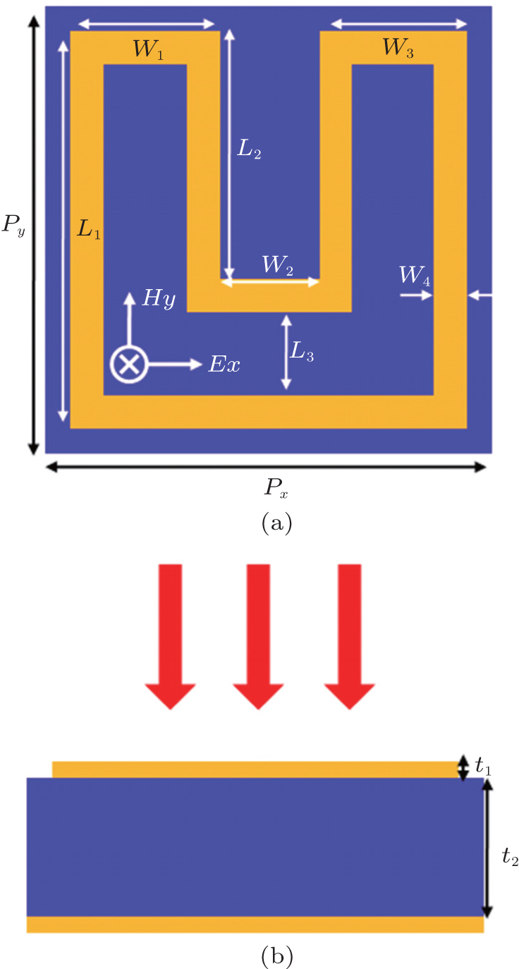 | Fig. 1. Schematics of metamaterial-based THz absorber: (a) U-shaped ring structure on the top of a polyimide spacer and one unit cell showing the direction of propagation of incident THz waves, and (b) cross-sectional view of the unit cell. The period (P) of unit cell is P = Px = Py = 27 μm. |
By employing the commercial finite-difference time domain (FDTD) software package (Lumerical FDTD solutions), the proposed MA is modeled and analyzed. The three-dimensional simulations are performed by a normally incident plane wave with the electric field parallel to the x axis. Periodic boundary conditions are employed for both x and y directions with a mesh step size of Δx = Δy = 0.25 μm, and a perfect matching layer boundary condition is employed in z direction with a mesh step size of Δz = 0.05 μm. The inset of Fig.
For impedance matching, the thicknesses of the metal and dielectric layer should be optimized so that the maximum absorption can be achieved. In simulations, the thickness of the top metal t1 = 200 nm, which has the same thickness as that of the ground metal plane. On the other hand, the thickness of the dielectric film also affects the absorption, because it influences the THz wave interaction between the adjacent metal layers. In the metamaterial THz absorber, the optimal thickness of polyimide layer (t2) is found to be t2 = 9 μm. Next, the structural parameters of the U-shaped ring are optimized so that the absorber achieves the highest absorption. The optimized geometric parameters are as follows in micrometers: L1 = 24, L2 = 15, L3 = 5, W1 = 9, W2 = 6, W3 = 9, and W4 = 2. These parameters are chosen in microscale so that the microstructure can be realized by the normal photolithography technology.
The simulated results of the S-parameters and absorption spectra of the proposed MA are shown in Fig.
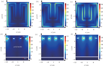
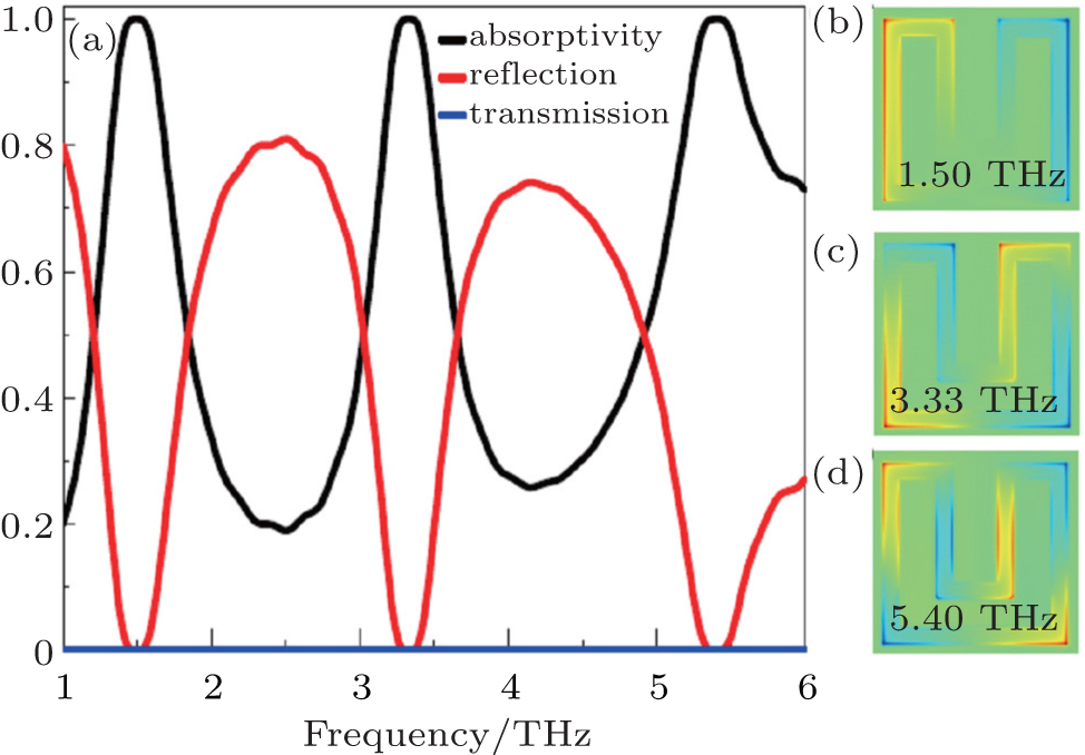 | Fig. 2. (a) Absorption spectra of the proposed MA. Distributions of the electric field [real(Ez)] in the top plane of the U-shaped metallic loop at frequencies of 1.50 THz (b), 3.33 THz (c), and 5.40 THz (d), respectively, for the x-polarization illumination. |
To understand the physical origin of the absorption peaks, we give the simulated normal components of electric field (Ez, in the top plane of the U-shaped metallic ring) distributions corresponding to the above mentioned three resonance frequencies (f1, f2, f3) in Figs.
According to our theoretical simulations, different order resonance absorption frequencies can be excited from the external THz field by the model of standing-wave plasmonic resonances. Under the electromagnetic wave illumination, the oscillation of the electrons within the metal film will be driven by the electrical field of the incident THz radiations to form localized surface plasmon; thus, positive and negative surface charges will be alternately accumulated at both sides of the edges of the U-shaped ring. Moreover, these electrons oscillating around the U-shaped ring form a kind of standing wave surrounding the ring. The lengths of the antinodes of the standing waves are mainly determined by the average perimeter of the ring, which explains why the frequencies of the resonance absorption peaks are perimeter related. In this case, the resonance responses of the absorber mainly depend on their average perimeter so that their characteristic resonance frequencies can be determined by the standing-wave model.[32] The frequency of the absorber is given by

To further understand the THz absorption behavior of the proposed MA, we also analyze the electric field |E| distribution in the structure. Figures
 | Fig. 3. The electric field (|E|) in the MA structure with a 9-μm thick polyimide spacer and x–z plane at y = 0 μm at frequencies of 1.50 THz (a) and (d), 3.33 THz (b) and (e), and 5.40 THz (c) and (f). |
In addition, the simulated power absorption distributions for the U-shaped metallic ring are shown in Figs.
 | Fig. 4. Energy dissipation in the MA structure with a 9-μm-thick polyimide spacer and x–z plane at y = 0 μm at frequencies of 1.50 THz (a) and (d), 3.33 THz (b) and (e), and 5.40 THz (c) and (f). |
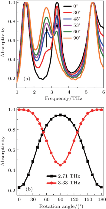
Furthermore, the simulated results for different incident polarization angles of the THz wave are shown in Fig.
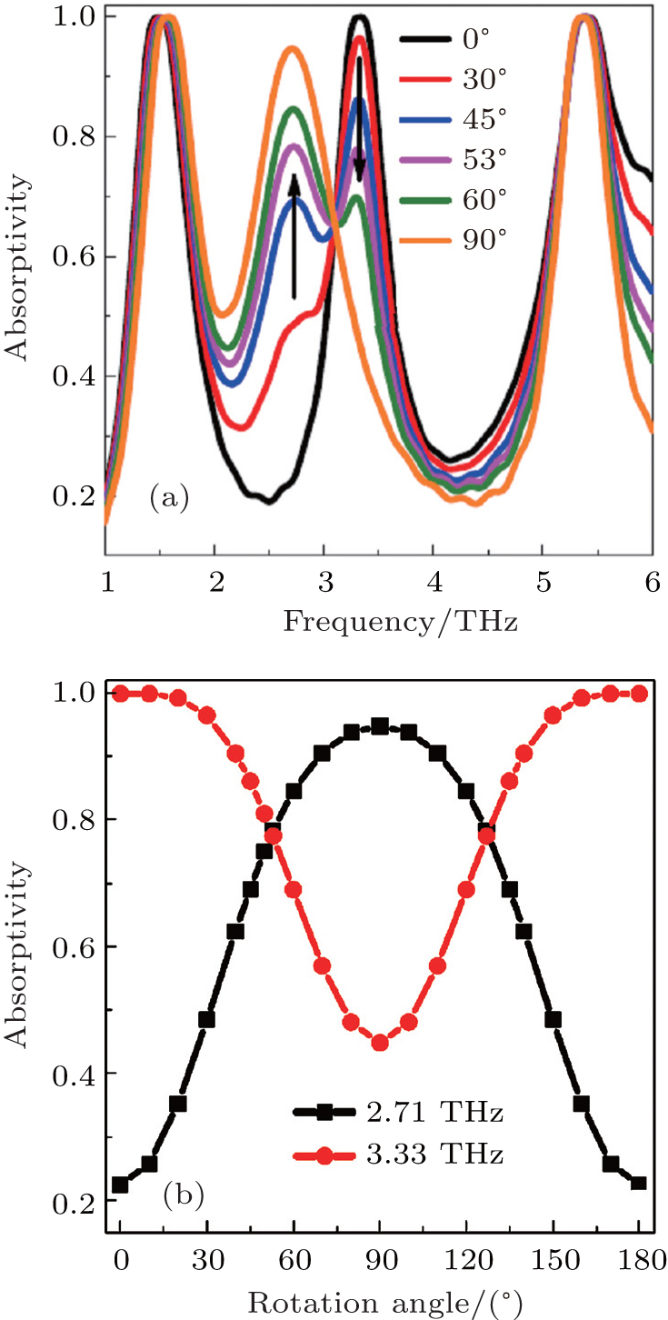 | Fig. 5. (a) Absorption spectra for different incident polarization angles of 0°, 30°, 45°, 53°, 60°, and 90°. (b) Maximum absorptivity as a function of the incident polarization angle for 2.71 THz and 3.33 THz, respectively. |
Fabrication errors cannot be avoided because the optimum design of the proposed MA cannot be perfectly fabricated in reality. To evaluate the effect of the fabrication errors on absorption, we take errors for three parameters: thickness of the dielectric layer (t2), the period (P), and the arm width (W4) of the U-shaped ring.
Here, we first discuss the effect of the dielectric layer thickness t2 on the absorption spectra. Figure
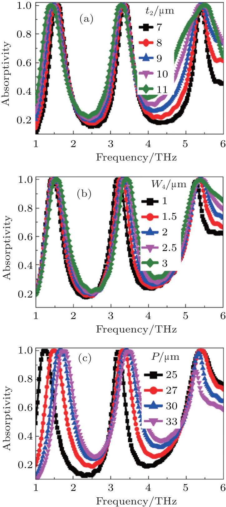 | Fig. 6. Absorption spectra of metamaterial absorber for the incident polarization angle of 0° at different parameters errors. (a) Absorption spectra in different dielectric thicknesses. (b) Absorption spectra with different linewidths. (c) Absorption spectra of unit cells with different periods. |
Next, we discuss the effect of the arm width W4 on the absorption spectra. Figure
Furthermore, we discuss the effect of the period P on the absorption spectra. Figure
Based on the above analysis, we can see that only the parameter P has a large influence on absorptivities of the absorption peaks. This is an advantage for the mask fabrication because less processing accuracy is required to fabricate the structure of the proposed MA.
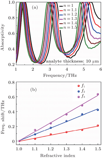
We next investigate the refraction index (RI) sensing of the proposed MA when the RI of the analyte changes but the thickness stays constant, as shown in Fig.
 | Fig. 7. (a) The transmission spectra of the proposed MA with 10-μm-thick analyte overlays, the RIs of the analyte are 1, 1.1, 1.2, 1.3, 1.4, and 1.5, respectively. (b) The redshifts of the three modes (f1, f2, and f3) versus the RI of the analyte. |
From Fig. 
In summary, we have designed a highly efficient THz multiband metamaterial absorber. Depending on the incident wave polarization, the absorber exhibits multifunctional application such as three-band, four-band, and broadband absorptions, which is useful in dynamically tuning the response of the absorber. In particular, the proposed MA can switch a narrow absorption band from 2.71 THz to 3.33 THz by rotating the device relative to the polarization direction from 90° to 0°. The high absorptivity of the proposed MA can be explained by the effect of the multipolar localized surface plasmon resonance enhancement. The error analyses of different structural parameters show that the error of the period has a great effect on the absorbing performance but the other two parameters have a slight effect. The proposed MA exhibits high refractive-index sensing sensitivity, which has potential applications in multi-wavelength sensing at THz frequencies.
| 1 | |
| 2 | |
| 3 | |
| 4 | |
| 5 | |
| 6 | |
| 7 | |
| 8 | |
| 9 | |
| 10 | |
| 11 | |
| 12 | |
| 13 | |
| 14 | |
| 15 | |
| 16 | |
| 17 | |
| 18 | |
| 19 | |
| 20 | |
| 21 | |
| 22 | |
| 23 | |
| 24 | |
| 25 | |
| 26 | |
| 27 | |
| 28 | |
| 29 | |
| 30 | |
| 31 | |
| 32 |