1. IntroductionRock-salt chalcogenides represent a significant group of functional materials, in which many novel properties are discovered, including superconductivity,[1] thermoelectricity,[2,3] ferroelectricity,[4] optoelectronics[5,6] and spintronics.[7,8] Recently, this class of materials has attracted considerable attention again due to the prediction and realization of the nontrivial topological properties in SnTe,[9,10] which is termed TCI.[11,12] In contrast to the widely studied Z2 topological insulator (TI),[13–20] Dirac cones lying on the topological crystalline insulator (TCI) surfaces are protected by the mirror symmetry, rather than time reversal (TR) symmetry. Therefore, TCI phase is associated with a new topological invariant called mirror Chern number, which classifies and distinguishes TCI from TI and an ordinary insulator. Importantly, a quantized π-Berry phase induced by the band inversion is needed and essential in TCI to characterize its topological properties such as Dirac cones.
Though the discovery of TCI enriches people’s understanding of the topological classification, few TCIs are realized in experiment. In order to satisfy the requirement of the potential device applications, it is urgent to find more TCIs, especially those with large band gap and high working temperature. As we all know, most lead chalcogenides adopt the same structure as SnTe, where the band inversion at L point is driven by the spin–orbit coupling (SOC). Considering that lead is much heavier than tin, it is natural to postulate that PbX may be a large band gap TCI due to the much stronger SOC. However, until now, no TCI phase is realized in PbX. Therefore, it is important to figure out the main factors of the band gap evolution in rock-salt chalcogenides with the purpose of achieving large band gap TCIs. Based on previous studies, there is a famous empirical relation[21] between band gap EG and lattice constant a0, which states that  has a linear relationship with
  for a series of relevant rock-salt semiconductors. However, this relation is invalid in lead chalcogenides, where PbTe exhibits a well-known anomaly that EG(PbS)> EG(PbTe)>EG(PbSe),[22,23] even though the lattice constant a0(PbTe) is much larger than a0(PbSe). This band gap anomaly has been a long-standing question and remains under debate.
In this paper, by combining ab initio calculations and TB method, we have studied the band evolution and band gap anomaly in PbX. Our studies show that the band gap anomaly in PbTe is closely related to the delocalized 5s electrons of Te. Comparing to S and Se, the 5s electrons of Te show much low binding energy (high on-site energy) and very extended distribution caused by the huge screening effect of the numerous interior electrons. As a result, Te 5s orbital pushes up the Pb p orbital through the huge s–p hybridization, leading to a large band gap for PbTe. Moreover, our calculations show that the SOC energy gap EG(PbPo) roughly agrees with the linear relation  formed by PbS and PbSe, and it is a negative number, which means that band inversion happens at L point in PbPo. Our detailed non-local Heyd–Scuseria–Ernzerhof (HSE) hybrid functional calculations show that PbPo is an indirect band gap semiconductor with a quantized π-Berry phase, which clearly indicates that PbPo is a TCI. The calculated mirror Chern number and surface states double confirm this conclusion.
This paper is arranged as follows. In Section 2, we will introduce the details of the ab initio calculations and TB model. In Section 3, based on the TB model, we will study the origin of the band gap anomaly. In Section 4, we will focus on the electronic structure and topological properties of PbPo. Finally, Section 5 contains a summary of this work.
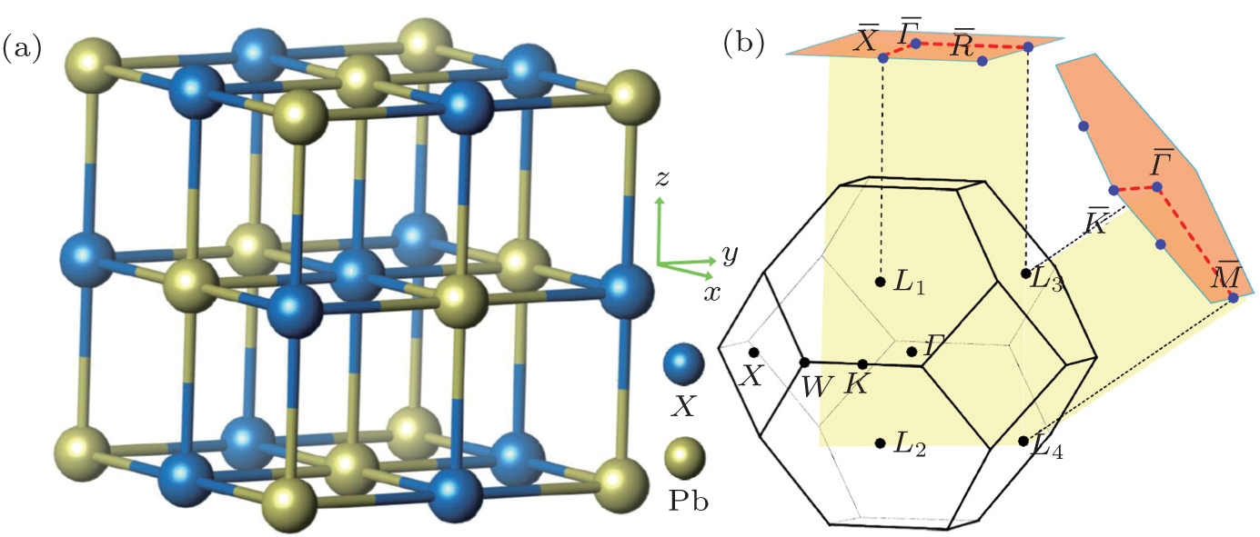
2. Ab initio calculations and TB methodOur ab initio calculations are carried out by the projector augmented wave (PAW) method[24,25] implemented in Vienna ab initio simulation package (VASP).[26,27] The crystal structure of PbX is shown in Fig. 1(a). Experimental lattice constants, with a0 = 5.942,[28] 6.124,[29] 6.460,[30] and 6.59 Å[31] for PbS, PbSe, PbTe, and PbPo are adopted in our calculations. The exchange and correlation potential is treated within the generalized gradient approximation (GGA) of Perdew–Burke–Ernzerhof type.[32] Considering the possible underestimation of the band gap by GGA, HSE hybrid functional[33] is further supplemented to improve the accuracy of the band gap. The cutoff energy of the plane wave expansion is 500 eV, and 11 × 11 × 11 k-point grids are used in the self-consistent calculations. SOC is consistently considered in the calculations. Modified Becke–Johnson (mBJ)[34] calculations are performed using the all-electron full-potential linearized augmented plane-wave (FP-LAPW) method implemented in the WIEN2k package.[35]
In order to study the band evolution and the band gap anomaly accurately, a general eight-band Slater–Koster[36] TB model with bases  is constructed, in which, besides the p–p hoppings, the s–p hybridizations are taken into account too

where
μ,
ν = cation, anion label the sublattices,
α,
β label the s, px, py, and pz orbitals,
i,
j label the unit cells,

represents the corresponding hopping parameters,

means the on-site energy of
α orbital on
μ sublattice,

creates (annihilates) an
α (
β) electron on
μ (
ν) sublattice at unit cell
i (
j). The interactions up to the fourth-nearest neighbors have been considered in this paper, which leads to a total of 32 independent parameters as listed in Table
1. The detailed definition of all those parameters and the way to get them will be given in the next section. We note that all parameters in Table
1 are reliable and very close to previous study.
[37] In momentum space, the Hamiltonian is given by

with
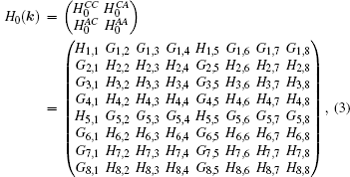
where
Hi,j and
Gi,j mean the matrix elements are real and imaginary numbers, respectively. The detailed descriptions of all matrix elements are given in the Appendix A.
When SOC is taken into account, the Hamiltonian size will be doubled. The final Hamiltonian with SOC can be written in the form
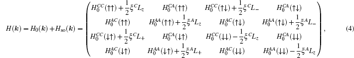
where
L± =
Lx± i
Ly.
Lx,y,z are the angular momentum operators,
ξC (
ξA) is the SOC parameter for cation (anion) p orbital. The typical literature SOC parameters
ξPb = 0.91 eV,
ξS = 0.05 eV,
ξSe = 0.22 eV,
ξTe = 0.49 eV, and
ξPo = 1.06 eV are adopted from Wittel’s spectral data
[38] in this paper.
Table 1.
Table 1.
 Table 1. Fitted TB parameters (in eV). .
|
PbS |
PbSe |
PbTe |
PbPo |
|
|
| A1 |
−1.1333 |
−2.0072 |
−1.6603 |
−2.2198 |
s,s(000) |
C−C |
| A2 |
0.0991 |
0.0891 |
0.0959 |
0.0857 |
s,s(110) |
C−C |
| A3 |
−0.0012 |
−0.0215 |
−0.0406 |
−0.0623 |
s,x(110) |
C−C |
| A6 |
7.7801 |
6.9910 |
7.2422 |
6.7530 |
x,x(000) |
C−C |
| A7 |
−0.0002 |
−0.0259 |
−0.0574 |
−0.0830 |
x,x(110) |
C−C |
| A8 |
−0.0169 |
−0.0283 |
−0.0419 |
−0.0535 |
x,x(011) |
C−C |
| A9 |
0.3623 |
0.3110 |
0.2693 |
0.2157 |
x,y(110) |
C−C |
| C1 |
−6.9050 |
−7.8493 |
−5.0836 |
−7.5326 |
s,s(000) |
A−A |
| C2 |
−0.0793 |
−0.0848 |
−0.0907 |
−0.0894 |
s,s(110) |
A−A |
| C3 |
0.1584 |
0.1689 |
0.1788 |
0.1875 |
s,x(110) |
A−A |
| C6 |
3.3582 |
3.1139 |
4.2744 |
4.2034 |
x,x(000) |
A−A |
| C7 |
0.1611 |
0.1686 |
0.1740 |
0.1810 |
x,x(110) |
A−A |
| C8 |
−0.0170 |
−0.0188 |
−0.0203 |
−0.0217 |
x,x(011) |
A−A |
| C9 |
0.1480 |
0.1356 |
0.1201 |
0.1106 |
x,y(110) |
A−A |
| B1 |
−0.1537 |
−0.1257 |
−0.1082 |
−0.0779 |
s,s(200) |
C−C |
| B2 |
0.0855 |
0.0974 |
0.1113 |
0.1247 |
s,x(200) |
C−C |
| B4 |
0.5301 |
0.4891 |
0.4579 |
0.4131 |
x,x(200) |
C−C |
| B5 |
0.1262 |
0.1050 |
0.0870 |
0.0605 |
y,y(200) |
C−C |
| E1 |
−0.2421 |
−0.2215 |
−0.1947 |
−0.1701 |
s,s(200) |
A−A |
| E2 |
−0.0854 |
−0.1308 |
−0.1733 |
−0.2168 |
s,x(200) |
A−A |
| E4 |
0.1210 |
0.1409 |
0.1516 |
0.1713 |
x,x(200) |
A−A |
| E5 |
0.0298 |
0.0330 |
0.0360 |
0.0393 |
y,y(200) |
A−A |
| D1 |
−0.6586 |
−0.6076 |
−0.5565 |
−0.5015 |
s,s(100) |
C−A |
| D2 |
1.3365 |
1.2714 |
1.2389 |
1.1757 |
s,x(100) |
C−A |
| D3 |
−1.6336 |
−1.4507 |
−1.4907 |
−1.2878 |
x,s(100) |
C−A |
| D4 |
1.8308 |
1.8474 |
1.8633 |
1.8795 |
x,x(100) |
C−A |
| D5 |
−0.2662 |
−0.2950 |
−0.3287 |
−0.3675 |
y,y(100) |
C−A |
| F1 |
0.3581 |
0.3100 |
0.2688 |
0.2239 |
s,s(111) |
C−A |
| F2 |
−0.0504 |
−0.0491 |
−0.0481 |
−0.0470 |
x,s(111) |
C−A |
| F3 |
−0.0071 |
−0.0069 |
−0.0067 |
−0.0065 |
s,x(111) |
C−A |
| F4 |
0.1154 |
0.1013 |
0.0868 |
0.0736 |
x,x(111) |
C−A |
| F5 |
0.0315 |
0.0425 |
0.0564 |
0.0680 |
x,y(111) |
C−A |
| Table 1. Fitted TB parameters (in eV). . |
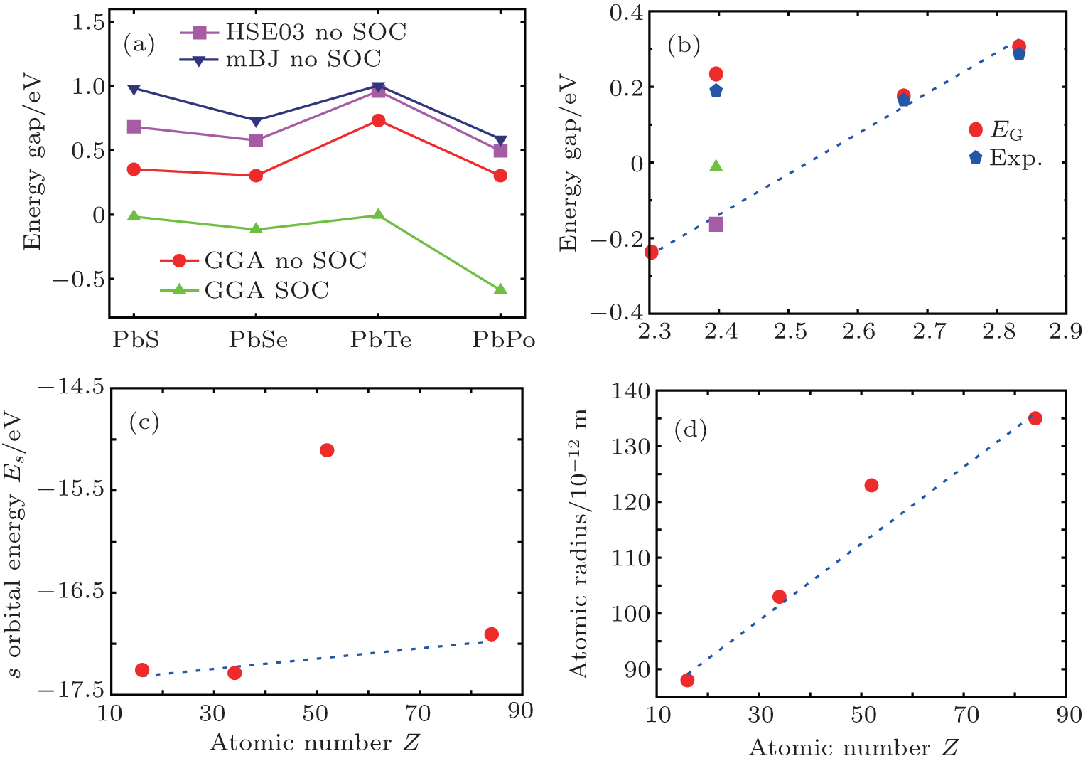
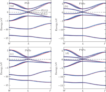
3. Band gap anomaly in PbXThe band gaps calculated by different methods for PbX are shown in Fig. 2(a), in which the non-SOC band gap is defined as 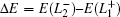 as shown in Fig. 3(a). In Fig. 2(a), the band gaps for PbTe show a distinct jump in all calculation methods, which means that the band gap anomaly in PbTe is intrinsic of the material, and irrelevant to SOC and the form of the exchange–correlation functional. As pointed out by Hummer et al.,[39] HSE03 is performing extremely well for lead chalcogenides. Therefore, in the following, the band structures calculated by HSE03 without SOC are taken as reference to fit the parameters in Eq. (3), and all parameters are directly transferred to Eq. (4) by adding the isotropic SOC term to estimate the band gaps and dispersions for all compounds. The comparisons between the non-SOC band structures obtained by Eq. (3) and original HSE03 calculations are shown in Fig. 3, and all fitted parameters are listed in Table 1, in which their detailed definitions are given in the sixth and seventh columns. Taking D3 as an example, “x,s(100)” and “C–A” mean D3 is the hopping parameter from the px orbital (x) of cation (C) to the s orbital (s) of anion (A) along the vector a0/2 (1,0,0). In Fig. 3, the non-SOC band structures obtained from HSE03 calculations and TB fittings by Eq. (3) are plotted with red lines and blue dots respectively. It is clear that our TB results agree with HSE03 calculations very well, which certifies that our model is accurate enough to study all details of the system.
The estimated band gaps EG (red circles) from Eq. (4) for all four compounds, as well as the experimental data at 4.2 K (blue pentagons), are summarized in Fig. 2(b). It is clear that our TB results almost overlap with the experimental data, which certifies that our model is accurate and powerful again. In order to study the origin of the band gap anomaly in PbTe, we have checked all the parameters in Table 1 carefully and found that the s orbital on-site energy of Te (C1) is obviously higher than the other three. Taking A1 (on-site energy of cation s orbital) as a referential energy, we get C1 − A1 equal to −5.7716, −5.8421, −3.4233, and −5.3128 for PbS, PbSe, PbTe and PbPo respectively. As a result, the band energy of Te 5s orbital at Γ point shown in Fig. 3(c) is about −13 eV, while it is nearly −15 eV for the other three compounds. Owing to this high on-site energy, Te 5s orbital will push up Pb 6p orbital through the s–p hybridization and result in a large band gap for PbTe. Now, we try to artificially decrease the on-site energy of Te 5s orbital and push down the band energy at Γ point until it reaches the “regular” level −15 eV as the other three. (For this purpose, C1 needs to be decreased by 2 eV.) After this adjustment, though the band gap does decrease about 0.2 eV as shown as the green triangle in Fig. 2(b), the band gap anomaly is still evident. Therefore, there must be some other reasons responsible to the band gap anomaly in addition to the high on-site energy of Te 5s orbital. We then recheck all the parameters in Table 1, and find that D3 also show some irregularity. Naturally, |D3| should decrease monotonically from PbS to PbPo due to the increasing lattice constant. However, |D3(PbTe)| is a little larger than |D3(PbSe)|, even though a0(PbTe) = 6.460 Å is obviously larger than a0(PbSe) = 6.124 Å. Based on the above discussions, after decreasing C1 by 2 eV and increasing D3 by 0.08 eV to a “regular” number, the final band gap for PbTe is shown as the purple square in Fig. 2(b), which falls on the line formed by PbS–PbSe–PbPo almost. Therefore, we conclude that the band gap anomaly in PbTe is mainly related to the high on-site energy of Te 5s orbital and the irregularly large s–p hopping.
Because SOC nearly has no contribution to the band gap anomaly as identified by our ab initio calculations, we would like to analytically discuss the band gap evolution and anomaly based on the non-SOC TB model in the following. At this case, the band gap ΔE can be easily written as
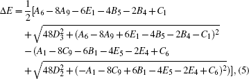
which shows an explicit relation between Δ
E,
C1, and
D3. In Eq. (
5), if we omit
D3, all
C1 (
E1) terms will cancel out each other, which means that the anomaly of
C1 needs the help of
D3 to be involved in the band gap formation and finally leads to a large gap for PbTe. Therefore, besides the directly bonded p–p hopping parameters (
A9,
C9, etc.), the key factors in determining the band gap for Pb
X are the huge s–p hybridization
D3 (
D2) and the irregular high on-site energy
C1. We note that such huge s–p hybridization is a typical character of the covalent systems rather than the ionic compounds. Generally, the hybridizations between the bonding (antibonding) states and non-bonding states are very weak in ionic compounds, such as Ca
X (
X = S, Se, Te), Sr
X (
X = S, Se, Te), and Ba
X (
X = S, Se, Te),
[40] in which the irregular high on-site energy of Te s orbital has negligible influence on the band gap
EG because the s (antibonding state from cation)-s (non-bonding state from anion) hybridization is negligible. This is the main reason why Ca
X, Sr
X, and Ba
X all obey the empirical relation

very well, even though the irregularity of the Te s orbital also exists in all these ionic systems. Moreover, we note that the s–p hybridizations
D3 (
D2) in lead chalcogenides are too strong to be treated by the perturbation method.
[41] Using the fitted parameters for PbTe to do a rough estimation,

is almost equal to (
A6 − 8
A9 + 6
E1 − 4
B5 − 2
B4 −
C1)
2. Therefore, the first square root in the right hand of Eq. (
5) is approximately equal to

which can be used to estimate the band gap evolution with
C1 and
D3 roughly.
Next, we would like to discuss the origin of the irregularity of C1 and D3 in depth. Because both C1 and D3 are closely related to the s orbital of anion, it is natural to propose that the irregularity may be originated from the chalcogen atoms themselves. We have calculated the binding energies of the outermost s electrons Es for all chalcogen atoms and plotted them with the atomic number Z in Fig. 2(c), in which the points for sulfur, selenium and polonium show an approximately straight line while the point of tellurium is much higher than the straight line. This result clearly demonstrates that the high on-site energy C1 of PbTe is inherited from the low binding energy of tellurium 5s electrons. To study the irregularity of D3 in PbTe, we show a plot of the atomic radius of the chalcogen atoms[42] as a function of atomic number Z in Fig. 2(d). We can see that the atomic radius of tellurium does not lie on the straight line as the others do and its position is higher than the line, which means tellurium 5s orbital is more extended. As a result, the hybridization between 5s orbital of Te and px orbital of Pb, i.e., D3, is abnormally larger than the “regular” value. Both the low binding energy and the extended distribution of the tellurium 5s electrons are related to the unusually strong screening effect of the V-period elements, as well as the penetration effect and relativistic effect. In general, the huge screening effect from the interior electrons will reduce the binding effect of nucleus and lead to a low binding energy and more extended distribution of Te 5s electrons. However, the detailed discussion of the atomic energy level and distribution are very complicated and out of the scope of this work. Finally, we claim that such 5s electrons’ irregularity is universal for the right side elements in the V row of the periodic Table of Elements,[43] e.g., Sn, and our discussion is universal for other covalent systems with the same structure. For example, similar analysis would give the conclusion that the 5s orbital irregularity of Sn will obviously reduce the band gap of the tin chalcogenides, which may be the main reason why the band gap of tin chalcogenide is usually smaller than the same row lead chalcogenide.[45,46]
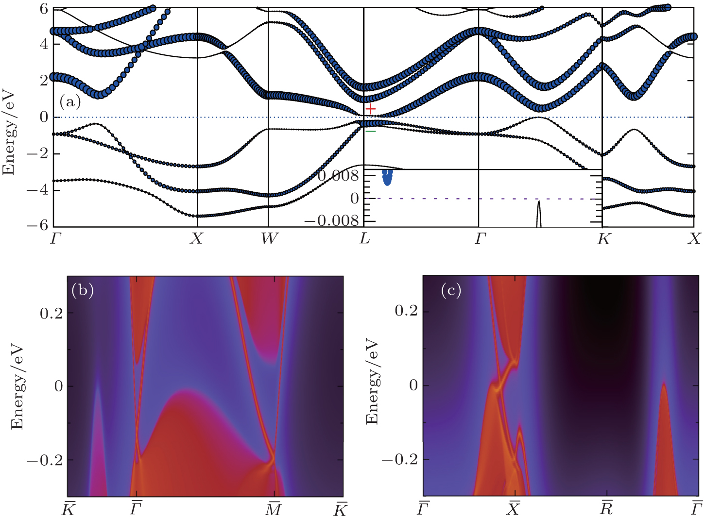
4. Topological properties in PbPoOne important result of our calculations is that EG is negative for PbPo as shown in Fig. 2(b), which means that band inversion happens at L point of PbPo. Detailed HSE03 + SOC calculations have been performed to confirm this conclusion. The calculated band structure is shown in Fig. 4(a), in which one p orbital of Pb is obviously dropped down below the Fermi level at L point as represented by the blue circles. Furthermore, our calculations show that PbPo is an indirect band gap (6.5 meV) semiconductor (see inset of Fig. 4(a)), rather than a direct band gap semiconductor[46] or semimetal.[47] All these band characters of PbPo are very similar to SnTe, which implies that PbPo may be a TCI too.
There are four L points {L1(0, π, 0), L2(0, 0, π), L3(π, π, π), L4(π, 0, 0)} in the first BZ of PbPo (see Fig. 1(b)). Because there are even band inversion points, the topological property of PbPo is different with 3D strong TI.[48,49] Actually, the topological property is protected by the mirror symmetry, and its topological invariant is the mirror Chern number CM instead of Z2.
The eigenvalue (m) of the mirror operator  is a good quantum number for PbPo, so we can classify the Bloch wavefunctions on
  plane by m, and define the berry connection Am
(k) and berry curvature Ωm(k) on the plane as follows:
plane by m, and define the berry connection Am
(k) and berry curvature Ωm(k) on the plane as follows:


where

with mirror eigenvalue
m = ±i is the
nth eigenstate at
k point. The sum is over all occupied bands. The mirror Chern number
CM is defined as
CM = (
n+i −
n−i)/2, where
nm = ∫
Ωm(
k) · d
S. Using the above formula, we find
CM = −2 for PbPo, which confirms that PbPo is a TCI. The other hallmark of the TCI is the mirror symmetry protected nontrivial surface states. We have calculated the surface states on (111) and (001) planes as shown in Figs.
4(b) and
4(c), respectively. As we can see, there are two distinct Dirac cones: one is pinned at the time reversal invariant momentum (TRIM) point while the other is situated off the TRIM point. On (111) plane,
L2,
L3, and
L4 are projected to the same point

while
L1 is projected to

point. There is no additional interaction coming from the scattering between odd
L-valleys, so the Dirac cones on (111) plane exactly locate at the TRIM points as shown in Fig.
4(b). On (001) plane,
L1 and
L2 (
L3 and
L4) are projected to the same point

(another

). The interaction between two
L-valleys will introduce an additional term to push the Dirac cones away from TRIM point.
[50] However,
k-points along

direction preserve mirror symmetry with respect to

operator. Therefore, even the Dirac cones are pushed away from TRIM point, they can still survive along

direction as shown in Fig.
4(c). The Dirac cones are protected by the mirror symmetry rather than TR symmetry, which is an important difference between TCI and
Z2 TI.
5. ConclusionIn summary, we have studied the band evolution in PbX, and found that, though the s orbital of the anion is far away from the Fermi level, it has crucial influence on the band gap through the huge s–p hybridization. The high on-site energy of Te s orbital and its irregular extended distribution combining together result in an irregular big band gap in PbTe, i.e., the famous band gap anomaly in lead chalcogenides. Furthermore, our calculations show that PbPo is an indirect band gap (6.5 meV) semiconductor with negative EG, which means that band inversion happens at L point in PbPo. The calculated mirror Chern number and surface states confirm that PbPo is a TCI.


 , Fang Zhong1, 2]