Shao Huai-Hua, Guo Dan, Zhou Ben-Liang, Zhou Guang-Hui. Velocity modulation of electron transport through a ferromagnetic silicene junction. Chinese Physics B, 2016, 25(3): 037309
Permissions
Velocity modulation of electron transport through a ferromagnetic silicene junction
Department of Physics and Key Laboratory for Low-Dimensional Structures and Quantum Manipulation (Ministry of Education), Hunan Normal University, Changsha 410081, China
Department of Physics and Electronic Science, Liupanshui Normal University, Liupanshui 553004, China
Project supported by the National Natural Science Foundation of China (Grant No. 11274108).
Abstract
Abstract
We address velocity-modulation control of electron wave propagation in a normal/ferromagnetic/normal silicene junction with local variation of Fermi velocity, where the properties of charge, valley, and spin transport through the junction are investigated. By matching the wavefunctions at the normal-ferromagnetic interfaces, it is demonstrated that the variation of Fermi velocity in a small range can largely enhance the total conductance while keeping the current nearly fully valley- and spin-polarized. Further, the variation of Fermi velocity in ferromagnetic silicene has significant influence on the valley and spin polarization, especially in the low-energy regime. It may drastically reduce the high polarizations, which can be realized by adjusting the local application of a gate voltage and exchange field on the junction.
Silicene, a monolayer of silicon atoms on a two-dimensional honeycomb lattice,[1] has recently been synthesized as a counterpart of graphene for silicon.[2–9] Compared to graphene, electrons in silicene also obey the Dirac equation around the K (K′) point of the Brillouin zone (BZ) at low energies.[10,11] However, silicene has a large spin–orbit coupling (SOC) which leads to the buckled structure between two sublattices, and the electronic structure is controllable by externally applying a perpendicular electric field. Many properties of silicene have been studied, such as electric-tunable band structure, topological transition,[12,13] and the effect of impurity adsorption.[14] Especially, the spin- and valley-dependent transport in silicene junctions has drown particular attention,[15,16] and the understanding on the transport property is meaningful to the design of a spintronic or valleytronic device based on silicene.
Meanwhile, it should be pointed out that silicene is usually synthesized on a substrate, whose stress influences the lattice constant of silicene.[2,4] In the low-energy model, the effect of nonuniform stress is shown by different Fermi velocities in different area of a silicene.[11] On the other hand, the suitable external stress, which is not so strong as to destroy the band type of Dirac cone,[17,18] may also stem from the attached ferromagnetic insulator or stretching and squeezing.[19–23] Therefore, the influence of the local variation of Fermi velocity on silicene-based spintronic/valleytronic applications is a very important issue.
In this paper, we study the charge, spin, and valley transport properties through a silicene sheet on substrate, on which the silicene is partly covered by a finite width ferromagnetic (FM) strip.[24,25] This may form a normal/FM/normal silicene junction with a variation of Fermi velocity in the FM-covered area of silicene. By matching the electron wavefunctions at the normal-ferromagnetic interfaces, we demonstrate that the variation of Fermi velocity in a small range can significantly enhance the total conductance while keeping the current nearly fully polarized, which may provide a experimental approach to detect the effect of substrate or ferromagnetic insulator on silicene. Further, the variation of Fermi velocity in ferromagnetic silicene has significant influence on the valley and spin polarization, especially in the low-energy regime. It may drastically reduce the high polarizations of the current, which can be realized by adjusting the local application of a gate voltage and exchange field on the junction.
2. Numerical methods
We consider a normal/FM/normal silicene junction as shown in Fig. 1, where the middle part of the silicene sheet is covered by an FM strip with width L. The effective low-energy Hamiltonian of the FM silicene is given by[10–13]
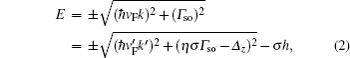
where vF is the Fermi velocity; (kx,ky) the wave vector; (τx,τy) the Pauli matrix in sublattice pseudospin space; Γso the strength of SOC; Δz is the onsite potential difference between two sublattices, which is tunable by externally applying a perpendicular electric field or by a gate voltage; η = ±1 corresponds to the K and K′ valleys; σ = ±1 denotes the spin indices; and h is the strength of exchange field in the FM region which may be induced by the magnetic proximity effect with a magnetic insulator EuS, as had been done for graphene.[23,26] The large value of Γso = 3.9 meV in silicene[11] leads to a cross correlation between valley and spin degrees of freedom, which is a clear distinction of silicene from graphene. For the Hamiltonian of the normal silicene region, we set Δz = h = 0 in Eq. (1).
In the tight-binding model,[11] where a = 3.86 Å is the crystal constant and t represents the transfer energy of usual nearest-neighbor hopping. The local stress from FM insulator and insulating substrate, or applied external stress to FM silicene, will affect the value of a and t, and change vF of a silicene. Moreover, we can also achieve the modulation of vF by transferring a spatial pattern from remote metallic layer via many-body velocity renormalization like in graphene.[27] The eigenvalues of Hamiltonians in the normal and FM silicene regions should be the same, i.e., the electron energy in the junction is given by
where k and k′ are the momenta in normal and FM regions, respectively, and is the changed Fermi velocity in the FM silicene.
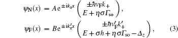
Let the x axis be perpendicular to the interface between two regions, as shown in Fig. 1, then the system has a translational invariance in the y-axis direction. If we ignore the plane wave of the y component, then the wavefunctions in each region can be written as
where
A, and B are coefficient constants for the wavefunctions.
Fig. 1. Schematic diagram of the model junction considered.
Assume that the interfaces are located at x = 0 and x = L, where L is the width of the FM silicene. To obtain the transport property through the junction, we should obtain the transmission coefficient at first. Considering the current conservation, we can obtain the boundary condition at the interfaces as
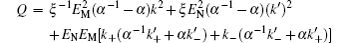
Taking into account boundary condition (4), from wavefunctions (3) we can finally evaluate the transmission probability
through the junction, where
with EN = E + ησΓso, EM = E + σh + ησΓso − Δz, and Since the lack of experimental and theoretical data, here we limit the range 0.2 ≤ ξ ≤ 5 referenced to the case in graphene.[27] Mostly, we are only interested in the vicinity of ξ = 1 for the problem.
Further, by setting kx = k cosθ and ky = k sinθ with incident angle θ, we can obtain the valley- and spin-dependent conductance
where with the junction transverse length Ly. Therefore, from Eq. (6) we can define total conductance G, valley and spin polarization Pv and Ps, respectively, as
which are dependent on the energy E, the width of FM strip L, and the ratio of Fermi velocities
3. Results and discussion
In what follows, we present some numerical examples of the spin- and valley-polarized conductances for the junction with and without the variation of Fermi velocity according to Eqs. (5)–(9), respectively. For convenience, we reduce all the physical quantities as dimensionless by introducing the units of energy E0 = 2Γso = 7.8 meV and characteristic length L0 = ħvF/E0 = 44 nm. Here, the parameters h = 0.3 and E = 1 are adopted.[15]
Figure 2 displays the valley- and spin-polarized conductances, GK↑ (solid line), GK′↑ (dotted line), GK↓ (dashed line), and GK′↓ (dash-dotted line), as a function of the FM strip width L for the junction of ξ = 1 with different electric field strength: Δz = 0.6 (Fig. 2(a)) and Δz = 1.5 (Fig. 2(c)), where figures 2(b) and 2(d) present the total conductance G (solid line), the valley polarization Pv (dashed line), and the spin polarization Ps (dotted line), corresponding to Figs. 2(a) and 2(c), respectively. Firstly, as seen in Figs. 2(a) and 2(b) for the weaker field case of Δz = 0.6, excepting for GK↓ other conductances display an oscillatory behavior with stable value as L increases, which makes a pretty large conductance G for the junction as the case in the graphene quantum well.[28] However, the two spin-down conductances are strongly suppressed, in particular GK↓ is suppressed to nearly zero as L increases further, which makes the spin polarization Ps averagely larger than 50% when L > 3. In contrast, as shown in Figs. 2(c) and 2(d) for the stronger field case of Δz = 1.5, excepting for GK↑ other conductances are strongly suppressed with the increase of L. As a result, both Pv and Ps reach up to nearly 100% in the wider L range and the current can be fully valley- and spin-polarized. Unfortunately, the total conductance G is small in this case, which is not suitable for device application. Further, both polarizations Ps and Pv for any field strength are very small as L < 1. In this case the contribution of imaginary waves (evanescent modes) to the conductance becomes larger but it is both spin and valley insensitive. The results here are in accord with some other published works.[15]
Valley- and spin-polarized conductances, GK′↑, GK↓, GK′↓, and GK′↓, as a function of L for (a) Δz = 0.6 and (c) Δz = 1.5. (b), (d) Total conductance Gc, the valley polarization Pv and the spin polarization Ps corresponding to panels (a) and (c), respectively.
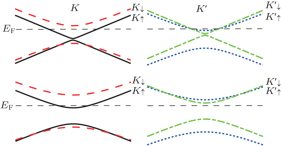
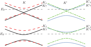
In order to understand the results shown in Fig. 2, the electron energy band structure near the K and K′ points calculated from Eq. (2) is demonstrated in Fig. 3 for the FM silicene. The upper panels of Fig. 3 correspond to the band structure for weak field Δz = 0.6, while the lower ones to those for strong field Δz = 1.5, where the horizontal dashed line denotes the Fermi energy level. As shown in the figure, the energy band is spin- and valley-resolved, while that for normal silicene is degenerate. For convenience here we denote K↑ (solid line), K↓ (dashed line), (dotted line), and (dash-dotted line), for subbands with different spin orientations and valleys. In the case of Δz = 0.6, the Fermi level does not cross subband K↓, hence the conductance GK↓ (dashed line in Fig. 2(a)) is almost zero in the range of L > 3. Meanwhile, the other three subbands, K↑, , and , all cross the Fermi level. This leads to the quite large corresponding conductances. As a result, the valley polarization Pv is very small (the dashed line in Fig. 2(b)), but the spin polarization Ps is pretty large. However, when the electric field strength is increased up to Δz = 1.5, the band gap for both the K and K′ valleys becomes larger, and the Fermi level only crosses subband K↑. This means that the current (conductance) through the junction is entirely carried by the states of K↑ subband in the range of L ≥ 3 and it is fully valley- and spin-polarized. However, the current is small because the transport channels from the other subbands are almost closed.[13,29] This is not suitable for spintronic/valleytronic device application, where a highly efficient spin- and valley-polarized current is needed. Therefore, we turn naturally to the question whether or not the variation of Fermi velocity in the FM silicene can improve this situation.
Fig. 3. The electron energy band structure near the K and K′ points for the FM silicene, where the upper panels correspond to the band structure for small Δz = 0.6, while lower ones to those for large Δz = 1.5, and the horizontal dashed line denotes the Fermi energy level.
Next, we investigate the effect of the variation of the Fermi velocity in the FM silicene on the electron transport through the junction. To avoid the influence of the imaginary waves, we take a rather large FM width L= 5. Figure 4(a) shows the valley- and spin-polarized conductances, GK↑ (solid line), GK′↑ (dotted line), GK↓ (dashed line), and GK′↓ (dash-dotted line) as a function of the ratio of Fermi velocity ξ. Figure 4(b) shows the valley polarization Pv and spin polarization Ps, as a function of the ratio of Fermi velocity ξ for the junction with Δz = 1.5. From the energy dispersion relation (2), we know that the change of the Fermi velocity can not move the energy band in longitudinal direction. As pointed above, the Fermi level still only crosses the K↑ subband. Then the current is entirely carried by the states of K↑ band in the region L > 3 and is fully valley and spin polarized. As shown in the figure, the conductances and the polarizations change in a large range of ξ. However, it is worth noting that, around ξ = 1, only the contributory conductance GK↑ still varies within a large range. Meanwhile, the spin and valley polarizations keep nearly 100%. It means that we can drastically increase the polarized current through the junction by changing the Fermi velocity of the FM silicene a little. This is just needed in spintronic or valleytronic application. Further, we also obtained some plots of valley- and spin-polarized conductances and the associated polarization of the junction with L = 0.5 as a function of the ratio of Fermi velocity ξ for different electric field strength, Δz = 0.6 and Δz = 1.5, respectively, which are not presented here because of the limitation of space. The result shows both spin and valley polarizations vary slowly around ξ = 1. In other words, the variation of Fermi velocity can not improve the low polarizations when L is small. However, for both L = 0.5 and L = 5, the conductances vary remarkably around ξ = 1. It means if the Fermi velocities of the normal and ferromagnetic silicenes are slightly unmatched, there will be a clear signal of electron transport. Importantly, one can detect the effect of substrate or extra FM insulator on a silicene by experimentally measuring the transport.
Fig. 4. (a) The valley- and spin-polarized conductances and (b) polarizations as a function of the ratio of Fermi velocity ξ for L = 5 and Δz = 1.5.
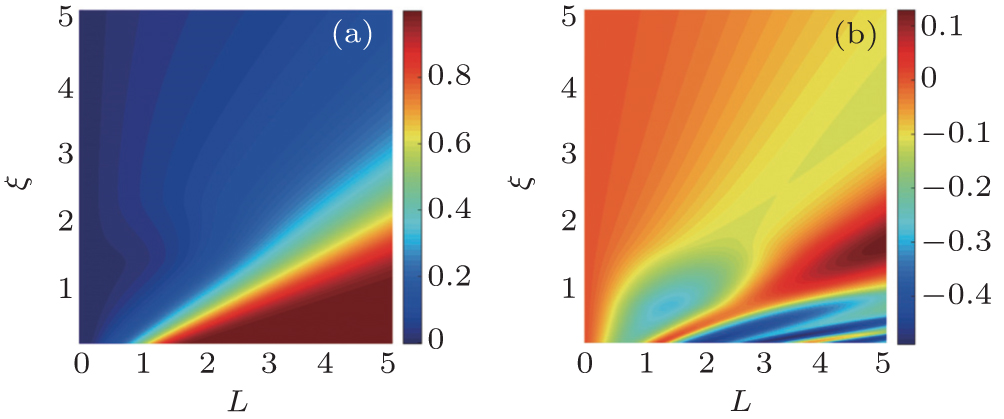
Furthermore, we turn to study the effect of the variation of the Fermi velocity on polarizations in FM silicene with different widths of the FM strip. Figure 5 shows the spin polarization Ps for Δz = 1.5 (Fig. 5(a)) and the valley polarization Pv for Δz = 0.6 (Fig. 5(b)), as a function of L and ξ, respectively. From Figs. 2(c) and 2(d) as well as the lower panels of Fig. 3, we know that the current will be fully spin and valley polarized (Ps > 0.95) for Δz = 1.5 and ξ =1 when L is over a critical value. As is shown in Fig. 5(a), this critical value is about L = 3. However, we find the variation of Fermi velocity can adjust the position of the critical line, with a proportional relation to the ratio of ξ and L. On the other hand, as shown by the dashed line in Fig. 2(b), there is no relatively high valley polarization ≥ 0.5 for Δz = 0.6 and ξ = 1. Figure 5(b) shows the valley polarization Pv mainly varies from −0.2 to 0.1 in most parameter region.
Fig. 5. (a) The contour plots of spin polarization Ps for Δz = 1.5 and (b) the valley polarization Pv for Δz = 0.6 as a function of L and ξ.
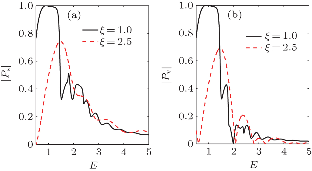
Finally, the conductances and their relevant polarizations are also functions of the energy E. Figure 6 shows the valley and spin polarizations Pv and Ps as a function of E for the junction with Δz = 1.5 and L = 5 for ξ = 1 and 2.5, respectively. From the comparison of the two velocity ratio cases, we can clearly see the change of Fermi velocity makes a hardly influence on the current polarization, especially in the low energy regime. Actually, it means that the polarized current which is obtained by adjusting local application of a gate voltage and exchange field may be hardly decreased by the change of Fermi velocity in the low energy regime. This effect must be fully considered in device design based on this system.
Fig. 6. (a) The spin polarization |Ps| and (b) the valley polarization |Pv| as functions of E with L = 5 and Δz = 1.5 for ξ = 1 and 2.5, respectively.
4. Conclusion
In summary, we have investigated the charge, valley, and spin transports in a normal/FM/normal silicene junction with varied Fermi velocity in the area of silicene covered by the FM strip. By matching the electron wavefunctions at the normal-ferromagnetic interfaces, it is demonstrated that the variation of Fermi velocity in a small range can largely enhance the charge conductance while keeping the current nearly fully polarized. Further, the variation of Fermi velocity can decrease the polarization of the current hardly in the low energy region. These results would be also applicable to other two-dimensional Dirac systems, such as monolayer of transition metal dichalcogenides.


 ]
]