Projcet supported by the National Natural Science Foundation of China (Grant Nos. 61404098, 61176070, and 61274079), the Doctoral Fund of Ministry of Education of China (Grant Nos. 20110203110010 and 20130203120017), the National Key Basic Research Program of China (Grant No. 2015CB759600), and the Key Specific Projects of Ministry of Education of China (Grant No. 625010101).
Abstract
Abstract
In this paper, the normally-off N-channel lateral 4H–SiC metal–oxide–semiconductor field-effect transistors (MOSFFETs) have been fabricated and characterized. A sandwich- (nitridation–oxidation–nitridation) type process was used to grow the gate dielectric film to obtain high channel mobility. The interface properties of 4H–SiC/SiO2 were examined by the measurement of HF I–V, G–V, and C–V over a range of frequencies. The ideal C–V curve with little hysteresis and the frequency dispersion were observed. As a result, the interface state density near the conduction band edge of 4H–SiC was reduced to 2 × 10¹¹ eV−1·cm−2, the breakdown field of the grown oxides was about 9.8 MV/cm, the median peak field-effect mobility is about 32.5 cm2·V−1·s−1, and the maximum peak field-effect mobility of 38 cm2·V−1·s−1 was achieved in fabricated lateral 4H–SiC MOSFFETs.
Due to excellent physical and electrical properties, such as high breakdown electric field, wide bandgap, high thermal conductivity, and high electron saturation velocity, silicon carbide (SiC) has attracted increasing attention in high-temperature, high-power, and high-voltage devices.[1–4] Metal–oxide–semiconductor field-effect transistors (MOSFETs) based on SiC have been regarded as a promising candidate for low-loss and fast power devices in advanced electronic systems.[5] Significant progress in 4H–SiC MOSFETs has been demonstrated recently, with the fabrication of accumulation-mode MOSFETs (ACCUFETs),[1] UMOSFET,[2,6] DMOSFET,[7–10] and RESURF MOSFET.[11] SiC lateral MOSFETs are also very attractive as high-frequency power transistors, which can favorably compete with Si lateral MOSFET.[11,12] SiC lateral devices have a distinctive advantage of being able to be integrated with other devices, reducing cost, and enhancing overall circuit performance.[11,13]
The growth of high-quality gate oxides (SiO2) with abrupt SiC/SiO2 interfaces, containing a low density of interface traps Dit, is crucial for the fabrication of reliable MOSFETs with high channel mobility on 4H–SiC.[14] The main source of the high Dit values has been attributed to residual carbon in the gate oxide layer,[15] which was observed in the form of clusters[16,17] distributed along the SiO2/SiC interface. Although the chemical nature of these clusters is still not completely understood, it has been related to carbon complexes and silicon oxycarbides (SiCxOy)[18] formed during the oxidation process. To form high-quality gate oxides with abrupt SiC/SiO2 interfaces, here a sandwich gate oxidation method[14] was used in our work. In this paper, our recent experimental work on N-channel enhancement lateral 4H–SiC MOSFFETs is reported. The lateral 4H–SiC MOSFFETs were successfully fabricated using ion implantation and sandwich (nitridation–oxidation–nitridation) type gate oxidation process. N-type MOS capacitors were also fabricated simultaneously with the lateral devices to investigate the interface properties of 4H–SiC/SiO2. The properties of 4H–SiC/SiO2 interfaces on N-type MOS capacitors were examined by the measurement of HF C–V, I–V, and G–V over a range of frequencies. High mobility of 38 cm2·V−1·s−1 was achieved for the fabricated lateral 4H–SiC MOSFFETs.
2. Experiments
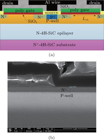
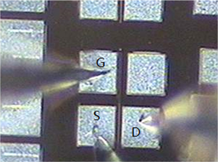
N-type 4°-off 4H–SiC (0001) Si-face epilayer with a net donor concentration of 6 × 1015 cm−3 was used to fabricate N-type MOS capacitors and lateral N-channel 4H–SiC MOSFFETs. A schematic cross section of the lateral N-channel 4H–SiC MOSFFETs and scanning electron microscopy (SEM) image of the fabricated device cross section are shown in Fig. 1. Figure 2 shows a top view photograph of a fabricated device with channel length of 10 μm and channel width of 200 μm. The P-well was formed by multiple-energy Al+ implantation of a box profile at three energies (40–350 keV). The N+ source and drain regions were created by nitrogen implantation of a box profile. The P+-region was also formed by high-dose Al+ implantation for obtaining good ohmic contacts on the p-well. After implantation, activation annealing was carried out in Ar at 1650 °C for 30 min. All wafers were protected with a carbon cap to minimize the surface roughness during annealing, and hereafter, the carbon cap was removed by low temperature thermal oxidation.
Fig. 1. (a) Schematic cross section of the fabricated lateral N-channel 4H–SiC MOSFFETs and (b) scanning electron microscopy (SEM) image (cross section) of fabricated device.
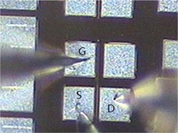
Fig. 2. Top-view of a fabricated lateral 4H–SiC MOSFET.
Prior to gate oxidation, the samples were prepared using RCA cleaning. The gate oxides were formed by the an NO/O2/NO sandwich-type process, which consists of a 2% NO pre-anneal for 1 hour, followed by the bulk oxide growth in 5% dry O2, finalized with a post oxidation anneal in 2% NO for an hour.[2] Next, a polysilicon film was deposited and patterned to form the gate contact. Finally, source and drain Ohmic contacts were formed by evaporating Ti/Ni/Al (50 nm/100 nm/200 nm) and annealing with rapid thermal processing (RTP).
Thicknesses of the gate dielectric films were determined by both scanning electron microscopy (SEM), and capacitance–voltage (C–V) measurements. The channel length (Lch) and width (Wch) of the fabricated lateral MOSFETs were 10 μm and 200 μm, respectively. The MOS capacitors and MOSFET electrical properties (transfer and output characteristics) were measured with the Agilent B1505A semiconductor characterization system. All measurements presented in this paper were performed at room temperature.
3. Results and discussion
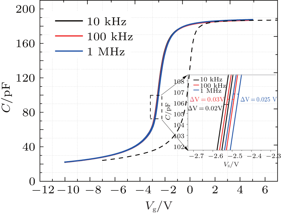
Figure 3 shows the bidirectional capacitance–voltage (C–V) characteristics measured with various frequencies from 10 kHz to 1 MHz for the MOS capacitor fabricated with NO/O2/NO sandwich oxidation. It can be seen that there is almost no hysteresis and frequency dispersion in the C–V curves. A relatively small hysteresis (about 0.025 V), corresponding to less border traps Nit near the interface (shown in Table 1), is observed in C–V curves. This is also confirmed by the conductance values, plotted in Fig. 4. For comparisons, the ideal C–V curve calculated using Poisson’s equation was also inserted in Fig. 3. It can be seen that the shape of the measured C–V curves is very similar to the theoretically calculated C–V curve (black dashed line), but there is a small voltage deviation between them, which indicates that there is relatively good quality of 4H–SiC/SiO2 interface.
Fig. 3. Bidirectional capacitance–voltage (C–V) characteristics measured with various frequencies from 10 kHz to 1 MHz for the MOS capacitor fabricated with NO/O2/NO sandwich oxidation.
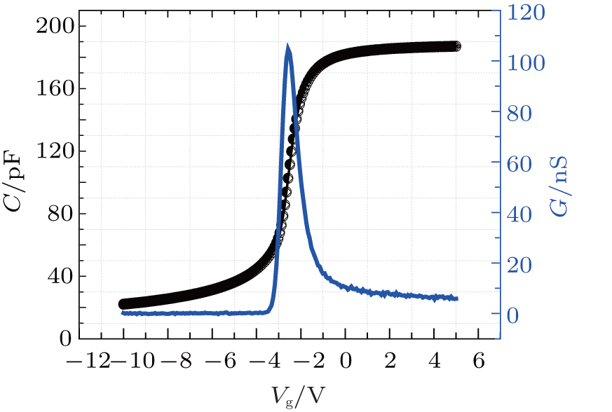
Fig. 4. Conductance–voltage (G–V) and capacitance–voltage (C–V) curves at 10 kHz for the MOS capacitor fabricated with NO/O2/NO sandwich oxidation.
Table 1.
Table 1.
Table 1.
Parameters of the MOS capacitor extracted from the C–V curve measured at 10 kHz.
.
Parameters
Value
Nit/cm−2
1.93 × 10⁸
ΔVFB/V
−0.71
Neff/cm−2
1.39 × 10¹¹
t/nm
58
Dit @0.2 eV/cm−2·eV−1
2 × 10¹¹
Table 1.
Parameters of the MOS capacitor extracted from the C–V curve measured at 10 kHz.
.
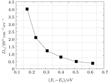
Table 1 lists the dielectric thickness (t), flat-band voltage shift (ΔVFB), effective dielectric charge (Neff) extracted from C–V measurements. Parameter t was calculated from the maximum accumulation capacitance (Cox). The Neff was obtained from (−ΔVFBCox)/qA, where ΔVFB is the VFB shift from the ideal value, A is the area of the capacitor, and q is the electronic charge. Figure 5 shows the distribution of interface state density (Dit) near the conduction band edge (Ec) of 4H–SiC estimated using the hi-lo C–V method. As shown in Fig. 5, the trap density (Dit) at 0.2 eV below the conduction band edge is as low as 2 × 1011 cm−2·eV−1, which indicates that NO/O2/NO sandwich-type process can reduce the interface state density significantly.
Fig. 5. Distribution of interface state density (Dit) near the conduction band edge (Ec) of 4H–SiC estimated using the hi-lo C–V method.
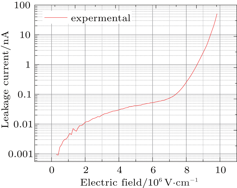
To evaluate the dielectric film breakdown characteristics, the typical current–electric field curves (I–E) of fabricated N-type 4H–SiC MOS structures is shown in Fig. 6, which is transformed from I–V curves. The electric field is approximated by (Vg–VFB)/t, where Vg and t are the gate voltage and the oxide thickness. From Fig. 6, it shows that the critical breakdown electric field of SiO2 is about 9.8 MV/cm at leakage current only 50 nA, and the statistical value of 20 measured MOS structures show that the median breakdown electric field is about 9 MV/cm.
Fig. 6. Typical current versus electric field (I–E) of fabricated N-type 4H–SiC MOS structure.
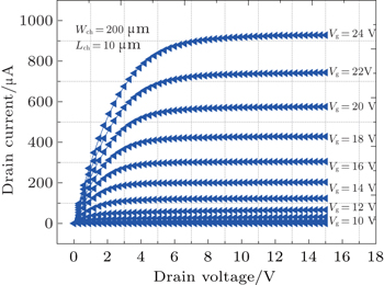
Figure 7 shows the typical output characteristics of the fabricated lateral enhancement mode N-channel MOSFET with the gate voltage (Vg) from 0 V to 24 V and the drain–source voltage (VDS) from 0 V to 15 V. The device exhibits a drain current of 900 μA at Vg = 24 V and VDS = 15 V. The output characteristics exhibit excellent linear and saturation region. Figure 8(a) shows transfer characteristics at room temperature for the fabricated devices measured at a drain voltage of 100 mV. The threshold voltage of 9.5 V is obtained by linear extrapolation from the linear region of the transfer characteristics. Figure 8(b) shows the transconductance versus the gate voltage Vg, in which a peak value of 3.68 μS is reached at gate voltage of 14 V.
Fig. 7. Typical output characteristics of the lateral enhancement mode N-channel MOSFET with gate voltage (Vg) from 0 V to 24 V and the drain–source voltage (VDS) from 0 V to 15 V.
Fig. 8. (a) Transfer characteristics of the fabricated devices measured at a drain voltage of 100 mV and (b) the corresponding transconductance characteristics.
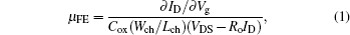
To examine the validity of the NO/O2/NO sandwich-type gate oxidation method, gate voltage dependence of the field-effect mobility μFE was measured, and the Vg for the measurement ranges from 0 to 20 V. The μFE can be calculated from the following formula using transconductance characteristic at the drain voltage of 100 mV:
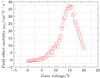
where Lch and Wch are the channel length and width, respectively, ID is the drain current, Ro is the contact resistance, and Cox is the oxide capacitance extracted from MOS capacitors. Figure 9 shows the field-effect mobility μFE as a function of gate voltage Vg in fabricated lateral MOSFETs. The mobility increases at low values of Vg, reaches a peak at the gate bias slightly higher than the threshold voltage, and then decreases. Maximum peak field-effect mobility of 38 cm2·V−1·s−1 was achieved. The statistic value of field-effect mobility μFE of 18 measured samples indicates that the median peak field-effect mobility is about 32.5 cm2·V−1·s−1. The results show that the sandwich gate oxidation method is helpful to reduce the interface defects and increase the channel mobility.
Fig. 9. Field-effect mobility μFE as a function of gate voltage Vg in fabricated lateral MOSFETs.
4. Conclusion
The normally-off N-channel lateral 4H–SiC metal–oxide–semiconductor field-effect transistors (MOSFFETs) have been fabricated using sandwich (nitridation–oxidation–nitridation) type process in this paper. The interface state density near the conduction band edge of 4H–SiC was reduced to 2 × 10¹¹ eV−1·cm−2, breakdown field of the grown oxides was about 9.8 MV/cm, and peak field-effect mobility of 38 cm2·V−1·s−1 was achieved. It is found that the NO/O2/NO sandwich-type oxidation process has a great potential as an alternative gate oxidation method in SiC MOS-based transistors.


 , Tang Xiao-Yan2, ‡,