
Theoretical investigation of structural and optical properties of semi-fluorinated bilayer graphene
[San Xiao-Jiao1, †,  , Han Bai2, 3, Zhao Jing-Geng1]
, Han Bai2, 3, Zhao Jing-Geng1]
|
|


† Corresponding author. E-mail:
Project supported by the Program of Educational Commission of Heilongjiang Province, China (Grant No. 12541131).
We have studied the structural and optical properties of semi-fluorinated bilayer graphene using density functional theory. When the interlayer distance is 1.62 Å, the two graphene layers in AA stacking can form strong chemical bonds. Under an in-plane stress of 6.8 GPa, this semi-fluorinated bilayer graphene becomes the energy minimum. Our calculations indicate that the semi-fluorinated bilayer graphene with the AA stacking sequence and rectangular fluorinated configuration is a nonmagnetic semiconductor (direct gap of 3.46 eV). The electronic behavior at the vicinity of the Fermi level is mainly contributed by the p electrons of carbon atoms forming C=C double bonds. We compare the optical properties of the semi-fluorinated bilayer graphene with those of bilayer graphene stacked in the AA sequence and find that the semi-fluorinated bilayer graphene is anisotropic for the polarization vector on the basal plane of graphene and a red shift occurs in the [010] polarization, which makes the peak at the low-frequency region located within visible light. This investigation is useful to design polarization-dependence optoelectronic devices.
The first experimentally obtained stable atomic monolayer material is graphene.[1,2] Due to its promising electronic mobility, robustness, and high crystal quality,[3–5] graphene has attracted a great deal of attention. However, its semimetallic nature is problematic with regard to developing usable graphene transistors and devices. Although there are abundant investigations on tailoring the material’s electronic properties in experiment and theory,[6–23] this field remains a major challenge. One alternative solution is to move to the multilayer derivatives.[6–9,24–27] For example, bilayer graphene has a gap tunable via chemical doping or by applying an external gate voltage.[24] Another method for changing the electronic properties of the material is via chemical functionalization of radicals, such as hydrogen,[12–17] oxygen,[18–21] and fluorine atoms,[28–34] which rehybridizes the C atoms from sp2 to sp3. Zhou et al. first investigated semi-hydrogenated graphene labeled graphone with a triangular hydrogenated configuration.[35,36] Their calculations indicated the ferromagnetism and a smaller band gap of ∼ 0.67 eV in this configuration.[36] As for the bilayer graphone, unlike the graphone sheet, the system is nonmagnetic but remains metallic.[27] Using geometry optimization, Feng and Zhang found the stable structure of semi-hydrogenated graphene with a rectangular hydrogenated configuration. The rectangular graphone is antiferromagnetic and has an indirect band gap of ∼ 2.45 eV.[17]
Furthermore, recent studies indeed clarified that bilayer graphene is also an interesting material on its own. Bilayer graphene exists in two stacking modifications, the AB stacking and AA stacking. Previously, most efforts have focused on the AB stacked bilayer graphene. Since 2009, the experimental realization of the AA-stacked graphene has been reported,[37,38] very limited theoretical investigations were focused on the AA-stacked bilayer graphene (AA-BLG).[38–42] The advantage of the AA-stacked graphene is the honeycomb pattern favorable for electron traffic, which is similar to that of an isolated graphene layer. An important feature of the AA-BLG is that the hole and electron Fermi surfaces coincide in the undoped material and such a band structure is unstable. The freestanding AA-BLG is a semiconductor with an indirect band gap of 0.91 eV.[41,42] Our interest on functionalized AA-BLG is driven to extend the family of graphene-based materials and to create materials with a direct band gap in the electronic band structure, which could be applied in electronics, optoelectronics, etc. As for the optoelectronics, the material is better with a direct or quasidirect band gap. To engineer the structural and electronic properties of the AA-BLG, we can dope it with appropriate dopants, choose the substrate, and apply a gate voltage, or apply a combination of these methods.[40] We have found another polymorphic form of one semi-fluorinated graphene and one unfluorinated graphene layer stacked in the AA sequence, where carbon atoms located in top positions and the two layers establish strong covalent bonds with a distance of about 1.62 Å. The semi-fluorinated graphene layer has a rectangular fluorinated configuration. The unfluorinated graphene layer forms double bonds (1.35 Å). The semi-fluorinated bilayer graphene is a wide gap semiconductor with a 3.46 eV direct band gap. Furthermore, the optical properties are calculated and the results indicate that the semi-fluorinated bilayer graphene is anisotropic for the polarization vector on the graphene plane and with the peak at the low-frequency region located within visible light in [010] polarization. The anisotropic features are unexpected in other graphene-related systems, such as graphite, graphene, and bilayer graphene. This investigation is useful to design polarization-dependence optoelectronic applications.
In order to investigate the structural and optical properties of semi-fluorinated bilayer graphene, we have carried out the following calculations. In the calculation of geometry relaxation and optical properties, density functional theory (DFT) calculations are performed with the CASTEP code[43] using the general gradient approximation[44] (GGA), Perdew–Burke–Ernzerholf (PBE) exchange correlation functional, and norm-conserving pseudopotential. In order to eliminate the interactions between graphene sheets, the vacuum space is set as 25 Å along the direction perpendicular to the carbon plane. The 8×8×1 k-points in the reciprocal space following the Monkhorst–Pack scheme are used. The structure is relaxed with a cutoff energy of 940 eV. No symmetry constraints are used. The convergences of energy and force are set as 10−6 eV and 0.01 eV/ Å, respectively. The phonon frequencies are calculated using the linear response technique within the CASTEP code.[43] Molecular dynamics simulations are performed using DFT within GGA[44] with the PBE parametrization as implemented in the DMol3 program.[45] All-electron treatment and double numerical basis including d- and p-polarization functions (DNP) are used. The convergence of energy in the self consistent field is set as 1 × 10⁻⁶ Hartree. The thermal stability of semifluorinated bilayer graphene is considered in the NVT ensemble with a Nose–Hoover thermostat at T = 300 K. Because hybrid functional calculations can give a more accurate band gap, the band gap is also calculated by using the Heyd–Scuseria–Ernzerhof 2006 (HSE06) approximation.[46]
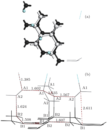
The optimized geometric structure of the semi-fluorinated bilayer graphene stacked in AA sequence is shown in Fig. 
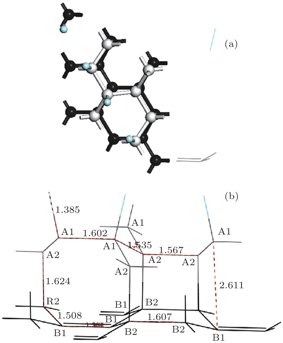 | Fig. 1. (a) Top and (b) side views of the semi-fluorinated bilayer graphene in AA configuration. Carbon atoms on top and bottom layers are colored with gray and black, respectively. Fluorine atoms are colored with blue. |
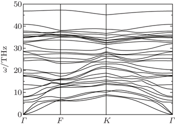
To confirm the dynamical stability of the semi-fluorinated bilayer graphene stacked in AA sequence, the phonon dispersion curves have been calculated (Fig.
 | Fig. 2. Phonon dispersion in the semi-fluorinated bilayer graphene. |
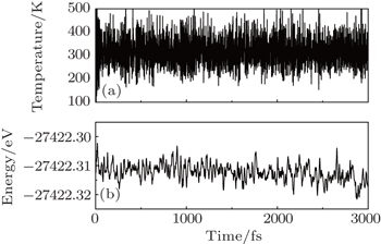
Furthermore, molecular dynamics simulations have been performed, applying the same method and parameter settings with Ref. [27]. The fluctuations of the temperature and potential energy in the semi-fluorinated bilayer graphene with AA configuration are plotted in Fig.
 | Fig. 3. Fluctuations of (a) temperature and (b) potential energy in the semi-fluorinated bilayer graphene as a function of time (step 1 fs) during MD simulation. |
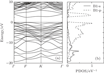
The optimized lattice parameters of the semi-fluorinated bilayer graphene are a = b = 5.10 Å. The semi-fluorinated bilayer graphene is a semiconductor with a 2.50 eV direct energy gap at the F point at the PBE level of theory as shown in Fig. 
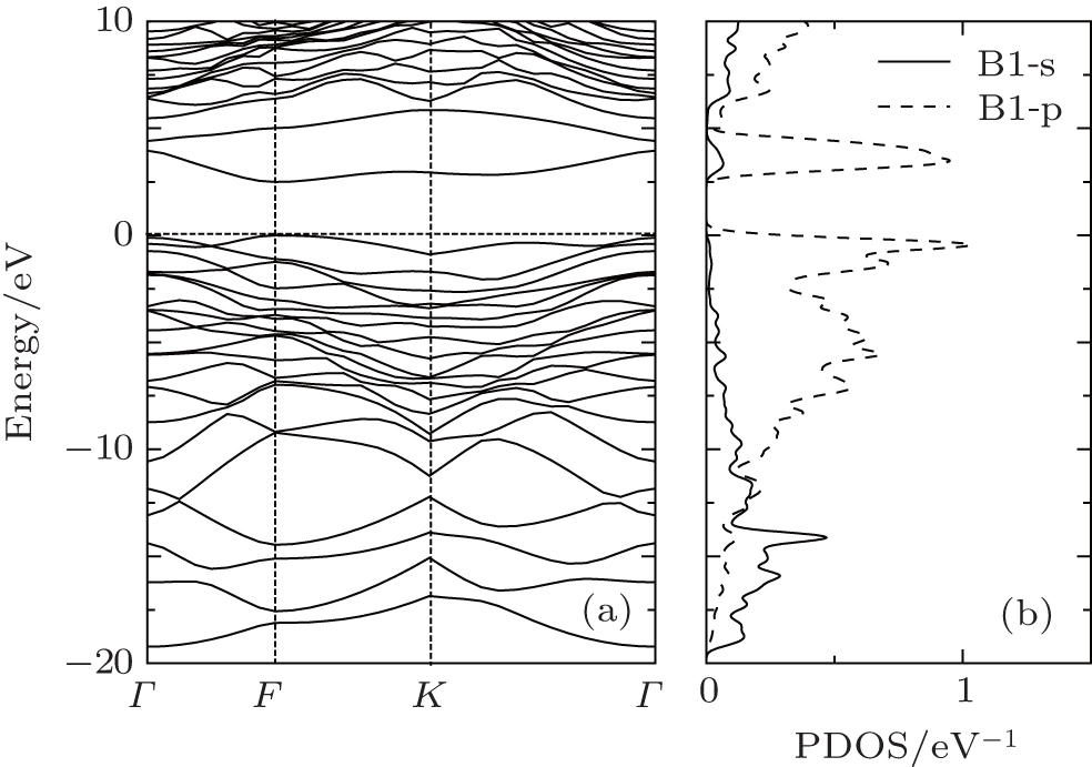 | Fig. 4. (a) Electronic band structure of the semi-fluorinated bilayer graphene together with (b) the partial density of states (PDOS) of carbon atoms (labeled B1) forming double bonds. |
When the interlayer distance is 1.62 Å, the two graphene layers in AA stacking can form strong chemical bonds. Under an in-plane stress of 6.8 GPa, this semi-fluorinated bilayer graphene becomes the energy minimum. Therefore, a possible way to induce the proposed semi-fluorinated bilayer configuration would be to apply an in-plane stress, maybe by growing epitaxially graphene layers on some appropriate substrate with enough lattice mismatch, as the case in AA-BLG.[41]
The optical properties of the semi-fluorinated bilayer graphene have been calculated and compared with those of the AA-BLG. In our calculations, the intraband contribution to the optical properties is not considered, which mainly affects the low energy infrared part of the spectra. In Fig.
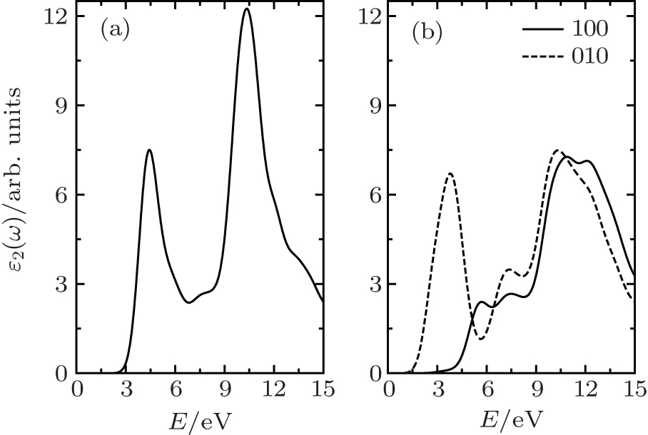 | Fig. 5. Calculated imaginary part of the dielectric function as a function of the photon energy for (a) AA-BLG and (b) semi-fluorinated bilayer graphene. |
There are a few good first-principles studies to date on the dielectric constants of 2D materials.[47–49] As mentioned in Ref. [47], quantum confinement is strong at small thickness, which gives rise to a very small ɛ2 in the low-energy range. Overall, the in-plane components (interband transition) of ɛ2 increase with increasing film thickness at all frequencies, conversing towards a constant value, while the general profile of the in-plane interband ɛ2 is consistent. In our calculation, for the dielectric functions ɛ2 presented in this work, we have first multiplied ɛ2 directly from CASTEP calculations by c = 25 Å and then divided it by the nominal film thickness h, where h is 4.95 Å and 5.96 Å for AA-BLG and semi-fluorinated bilayer graphene, respectively (h is the sum of the thickness of graphene (3.35 Å) and the corresponding bulk).
The result of AA-BLG is plotted in Fig.
In this work, the structural and optical properties of the semi-fluorinated bilayer graphene have been investigated. Our calculations indicate that the semi-fluorinated bilayer graphene with AA stacking sequence and rectangular fluorinated configuration is dynamically stable and can be maintained at room temperature. When the interlayer distance is 1.62 Å, the chemical bonding occurs, the system is formed by 8×4 membered rings. Under an in-plane stress of 6.8 GPa, this semi-fluorinated bilayer graphene becomes the energy minimum. The semi-fluorinated bilayer graphene is a semiconductor with a 3.46 eV direct band gap at the F point. The p electrons from the B1 atoms are mainly responsible for the electronic behavior at the vicinity of the Fermi level. Furthermore, the semi-fluorinated bilayer graphene is anisotropic and has a peak at the low-frequency region located within visible light in the [010] polarization.
| 1 | |
| 2 | |
| 3 | |
| 4 | |
| 5 | |
| 6 | |
| 7 | |
| 8 | |
| 9 | |
| 10 | |
| 11 | |
| 12 | |
| 13 | |
| 14 | |
| 15 | |
| 16 | |
| 17 | |
| 18 | |
| 19 | |
| 20 | |
| 21 | |
| 22 | |
| 23 | |
| 24 | |
| 25 | |
| 26 | |
| 27 | |
| 28 | |
| 29 | |
| 30 | |
| 31 | |
| 32 | |
| 33 | |
| 34 | |
| 35 | |
| 36 | |
| 37 | |
| 38 | |
| 39 | |
| 40 | |
| 41 | |
| 42 | |
| 43 | |
| 44 | |
| 45 | |
| 46 | |
| 47 | |
| 48 | |
| 49 |