Mechanism of floating body effect mitigation via cutting off source injection in a fully-depleted silicon-on-insulator technology
Huang Pengcheng1, Chen Shuming1, 2, †,  , Chen Jianjun1
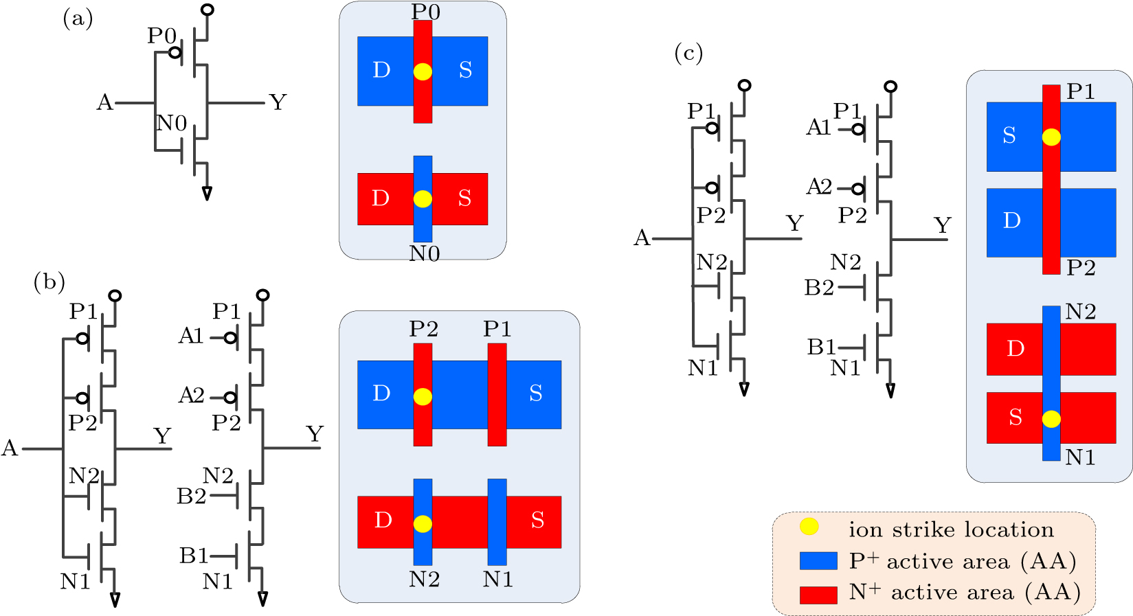
, Chen Jianjun1 Three layout structures for an inverter, (a) the conventional layout, (b) the conventional layout of stacking transistors, (c) the proposed in-line stacking layout of stacking transistors. Here, P0, P1, P2 represent PMOS transistors, while N0, N1, N2 represent NMOS transistors.