Mechanism of floating body effect mitigation via cutting off source injection in a fully-depleted silicon-on-insulator technology
Huang Pengcheng1, Chen Shuming1, 2, †, , Chen Jianjun1
College of Computer, National University of Defense Technology, Changsha 410073, China
National Laboratory for Parallel and Distributed Processing, National University of Defense Technology, Changsha 410073, China


† Corresponding author. E-mail: smchen_cs@163.com

Project supported by the National Natural Science Foundation of China (Grant Nos. 61376109, 61434007, and 61176030) and the Advanced Research Project of National University of Defense Technology, China (Grant No. 0100066314001).

Abstract
Abstract

In this paper, the effect of floating body effect (FBE) on a single event transient generation mechanism in fully depleted (FD) silicon-on-insulator (SOI) technology is investigated using three-dimensional technology computer-aided design (3D-TCAD) numerical simulation. The results indicate that the main SET generation mechanism is not carrier drift/diffusion but floating body effect (FBE) whether for positive or negative channel metal oxide semiconductor (PMOS or NMOS). Two stacking layout designs mitigating FBE are investigated as well, and the results indicate that the in-line stacking (IS) layout can mitigate FBE completely and is area penalty saving compared with the conventional stacking layout.

1. Introduction

Silicon-on-insulator (SOI) technology is widely used in aerospace applications for its intrinsic hardness towards radiation effects, especially its reduced single event upset (SEU) effects[14] as well as its single event latchup (SEL) immunity compared with bulk counterparts. The reduced single event sensitivity is mainly from the reduced charge collection depth, and the generated single event transient (SET) pulse width is usually less than 100 ps.[57]

The study of SET in SOI technology is still widespread, and the mitigation of SET is still of great concern, because serious propagation-induced pulse broadening (PIPB) effect in SOI technology can broaden the generated SET of small width to several ns.[5,6,8] In general, floating body effect (FBE)[911] is considered as the most important SET generation mechanism in SOI technology, and body-tie[1214] is usually used to mitigate FBE as well as the generated SET pulse width. However, the mitigation from body-tie is limited, and it can only mitigate the SET pulse width about several or several tens of picoseconds.[7,12]

In this paper, based on the investigation into the mechanism of FBE, we proposed a novel layout-level in-line stacking (IS) technique to mitigate FBE in SOI technology. Three-dimensional technology computer-aided design (3D-TCAD) mixed-mode simulations were performed to investigate its effectiveness. The simulation results indicated that it can mitigate FBE completely and then mitigate the generated SET completely as well. The gist of this layout-level technique is to cut off the source injection in SOI transistors, so that the FBE is cut down completely, and then the charge collection in the drain is reduced greatly.

2. In-line stacking technique

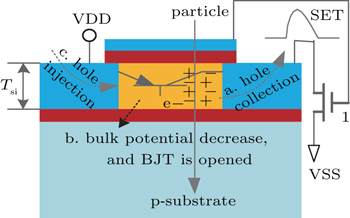
In the bulk complementary metal oxide semiconductor (CMOS) process, the well-structures for positive-channel metal oxide semiconductor (PMOS) and negative-channel metal oxide semiconductor (NMOS) are different. However, the well-structures for PMOS and NMOS in SOI process become similar. As shown in Fig. 1, for a PMOS transistor, the volume of the bulk region (i.e., the channel region) is far smaller than that in bulk CMOS process, which is WpLpTsi (Wp is the width of PMOS, Lp is the channel length of PMOS, and Tsi is the thickness of the silicon film). Obviously, in the bulk region, the amount of electrons or holes is limited, so that the bulk potential is easily changed by additional charge left in the bulk region.

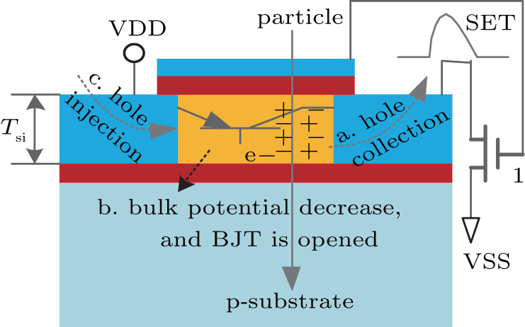
Fig. 1. The cross-section of a SOI PMOS transistor, and the sketch map of the mechanism for floating body effect.

If the off-state PMOS is struck by a particle, a large amount of electron–hole pairs are deposited along the track. As shown in Fig. 1, the deposited holes are collected by the drain gradually due to the drain electrical field, and the electrons are left in the bulk region. Because of the small size of the bulk region, the remaining electrons will decrease the bulk potential greatly. In this case, as shown in Fig. 1, the parasitic bipolar junction transistor (BJT) will be open, and a large amount of holes are injected from source, that is the floating body effect occurs. Because Tsi is only of several tens of nanometers, the deposited electrons or holes in the bulk region are also limited, however, the charge collection in the drain is far larger than the deposited charges due to FBE, and it is large enough to cause a SET in general.

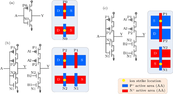
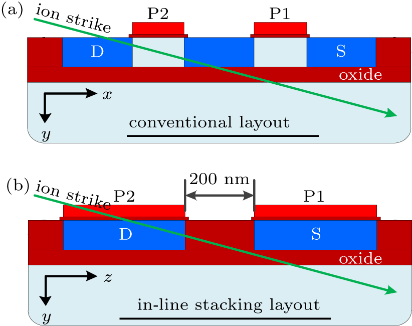
In order to mitigate the source injection, except for adding body-tie, dividing the parasitic BJT into two tandem BJTs is somewhat effective, for the two BJTs may not be opened simultaneously. In circuit design, as shown in Fig. 2, copying the transistor and connecting them in series can induce the stacking transistors structure, which can help to implement this scheme. For those NOT-like logic cells, they are of stacking transistors themselves, as shown in Fig. 2(b), the circuit does not need this rad-hardened design anymore.

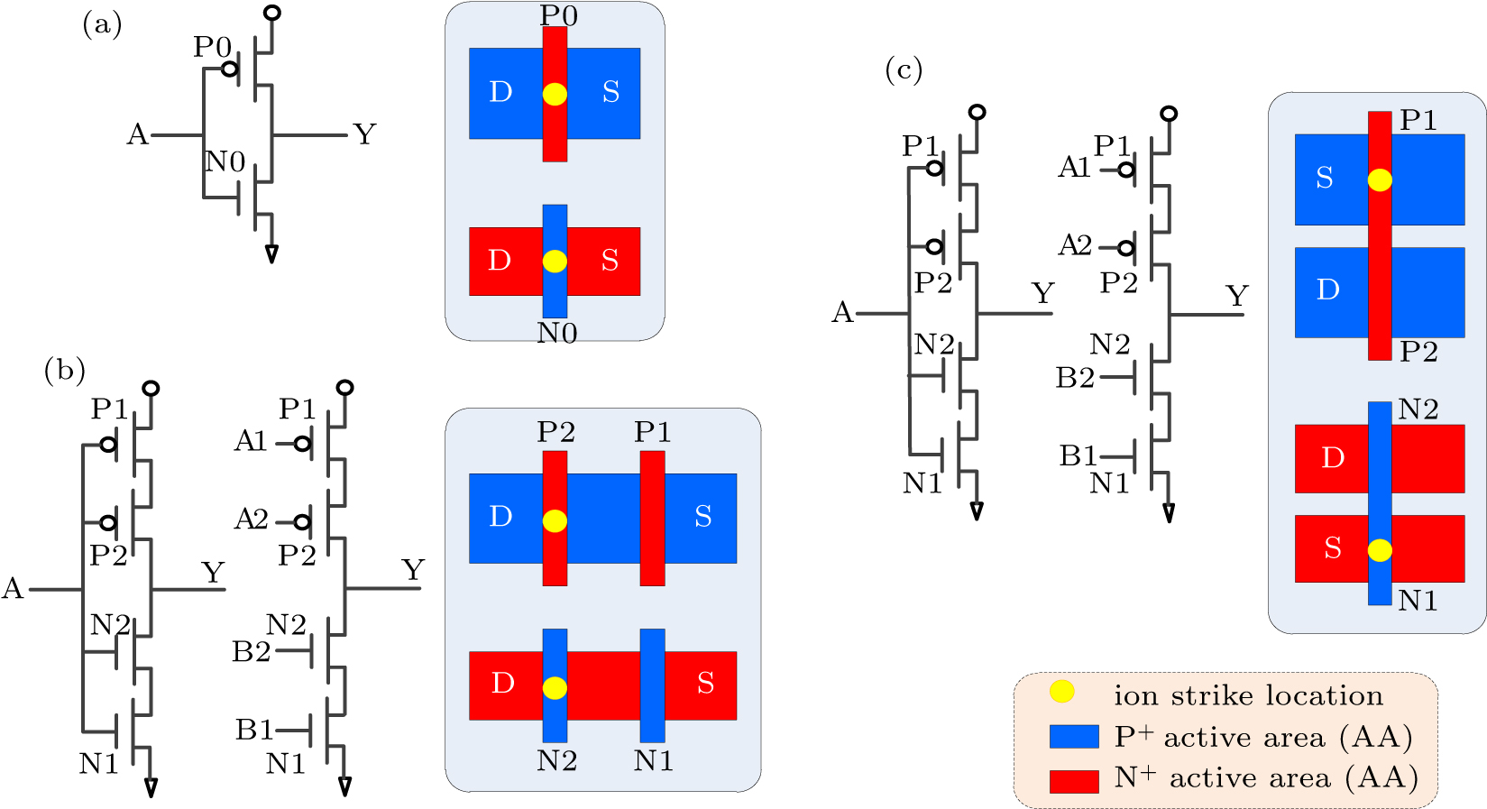
Fig. 2. Three layout structures for an inverter, (a) the conventional layout, (b) the conventional layout of stacking transistors, (c) the proposed in-line stacking layout of stacking transistors. Here, P0, P1, P2 represent PMOS transistors, while N0, N1, N2 represent NMOS transistors.

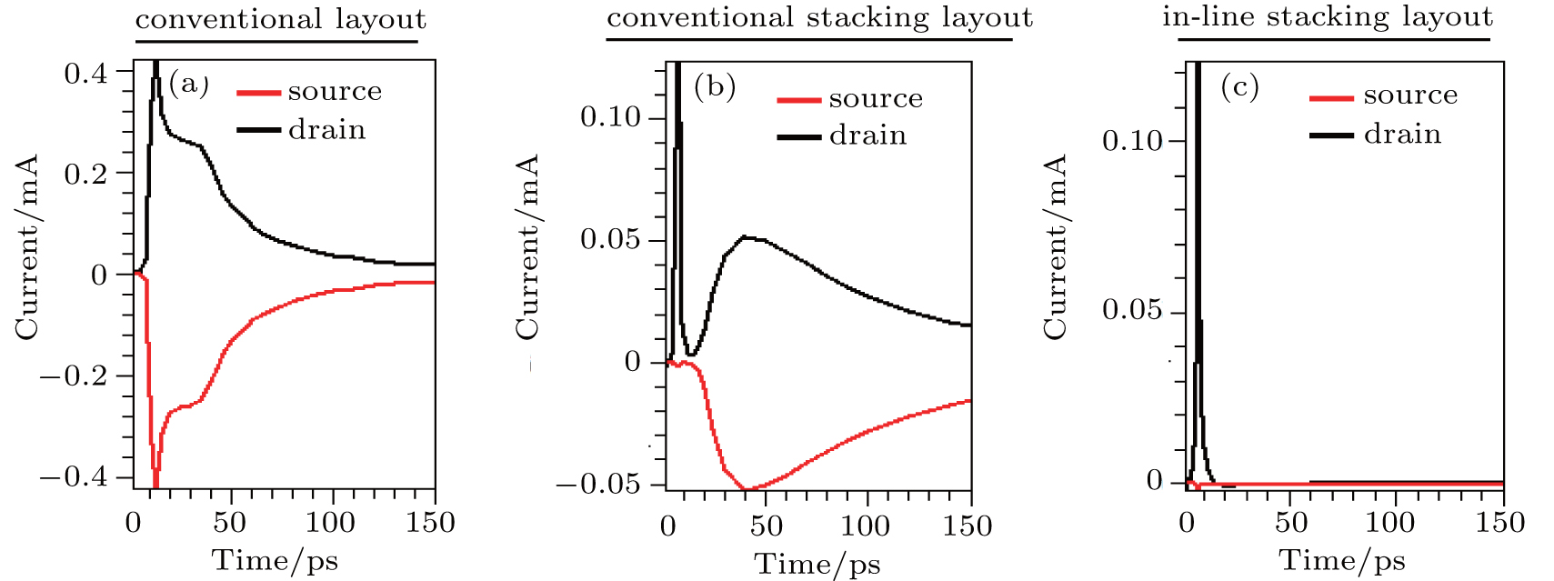
Two parasitic BJTs in the layout shown in Fig. 2(b) are still likely to be opened simultaneously if they are hit by heavy ions successively. In order to reduce the probability of a successive hit on two parasitic BJTs, in-line stacking layout of stacking transistors are proposed, which is shown in Fig. 2(c). In this case, the distance of two parasitic BJTs is increased ≥ 1 times, so that they are unlikely to be struck simultaneously.

3. Simulation setup

For an inverter in 40-nm FD-SOI technology, the channel lengths of PMOS and NMOS are 40 nm, and the widths are 450 nm and 300 nm, respectively for PMOS and NMOS. Because 3D-TCAD simulation is widely used for investigating the mechanism of single event charge collection, we employ Synopsys TCAD vF-2011.09 to have P-hit and N-hit mixed-mode simulation. As shown in Fig. 3, the PMOS and NMOS are built into TCAD model to study FBE mechanism. The thickness of the buried oxide is 15 nm, and the thickness of the silicon film (i.e., Tsi) is 20 nm. According to design rules, the space in z direction between two transistors in in-line stacking layout should be larger than 110 nm, and it is set as 200 nm here.

Fig. 3. Simulated structure for 40-nm FD-SOI PMOS in an inverter. (a) P-hit simulation, (b) N-hit simulation.

The same as with our previous works,[1520] heavy-ion strike is modeled with an electron–hole pair column, which is a Gaussian radial profile with a characteristic 1/e radius of 50 nm and a Gaussian temporal profile with a characteristic decay time of 0.25 ps. The ion strike is set at 10 ps. The ion track acts as the axis of the electron–hole pair column, and the LET value is kept constant along the ion track. The mixed-mode simulations are performed at room temperature with the voltage supply of 0.9 V. For P-hit simulation, the input of the inverter ‘A’ is biased to logic ‘1’ so that PMOS is in off-state. For N-hit simulation, ‘A’ is biased to logic ‘0’. The ion strike location is the center of the gate for it is the most sensitive district for the TCAD devices. The normally incident ion LET was varied from 20 MeV·cm2/mg to 80 MeV·cm2/mg.

The physical models employed are listed as follows: 1) Fermi–Dirac statistics; 2) the effect of doping-dependent SRH recombination and Auger recombination; 3) the effect of band-gap narrowing; 4) the impact of temperature, doping, electric field, and carrier–carrier-scattering on mobility; and 5) a hydrodynamic carrier transportation model. If other than specified, the default models and parameters provided by Sentaurus TCAD vF-2011.09 are used.

4. Simulation results analysis
4.1. P-hit simulation

As ions strike the gate center of the off-state PMOS (P0 or P2 in Fig. 1) in an inverter with LET of 20 MeV·cm2/mg, an obvious SET is generated at the drain in the conventional layout, which is shown in Fig. 4. In the conventional layout, the generated SET pulse width is about 15 ps. However, in the two stacking layouts, no SET comes into being. Thus, the circuit structure with stacking transistors is beneficial for SET mitigation in FD-SOI technology.

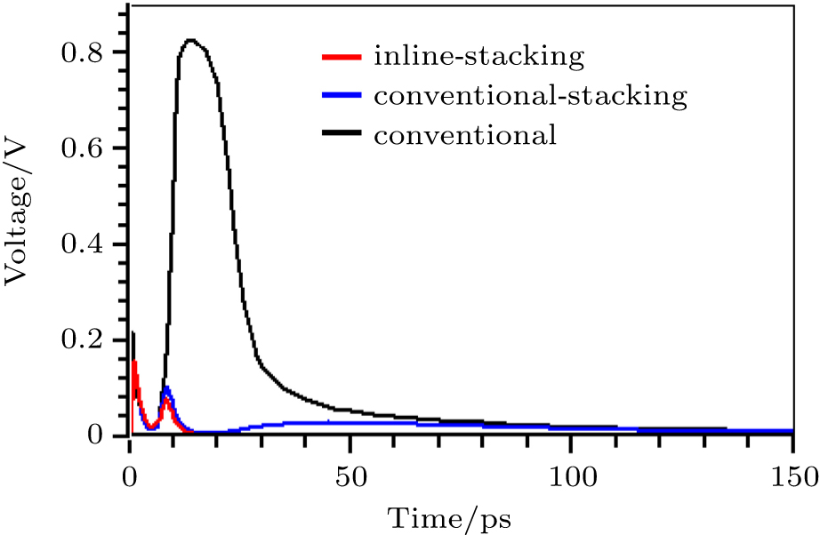
Fig. 4. P-hit SET with ion strike at gate center of off-state PMOS (P0 or P2 in Fig. 1) with the LET of 20 MeV·cm2/mg. The ion strike is at 10 ps (unless otherwise specified, the same as that in other figures).

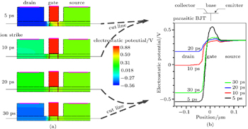
What is the reason for SET in FD-SOI technology? Is it caused by FBE? In Fig. 5, the current transient can help us to have a better understanding. For P0 in Fig. 1, as shown in Fig. 4(a), there are large and reverse current transient at drain and source, which indicates that FBE is distinct and can bring about a large amount of source injection in FD-SOI technology. In general, the peak of the drain current is caused by carrier drift. However, the peak in Fig. 5(b) is less than that in Fig. 5(a), which indicates that the carrier drift is enhanced by FBE though it is the origin of FBE in Fig. 5(a). In addition, their total is 0 except for a while near ion-strike, which also indicates that FBE has enhanced carrier drift. Because carrier drift is not enhanced by FBE in Fig. 5(b) and then no SET generated, SET in FD-SOI technology is not the product of carrier drift/diffusion, and FBE is the absolute dominant cause for SET in FD-SOI technology.

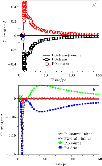
Fig. 5. P-hit current transient with ion strike at gate center with the LET of 20 MeV·cm2/mg, (a) for off-state P0 in Fig. 1, (b) for off-state P2 in Fig. 1.

In Fig. 5(b), we can see that the current transient at drain and source are reduced greatly by stacking transistors, which indicates that a parasitic BJT being divided into two BJTs is effective for mitigating FBE. For conventional stacking layout, there is still about 50 μA source injection, however, for in-line stacking layout, no source injection exists, therefore, the in-line stacking layout does better in mitigating FBE. Certainly, we can still see that there is a current peak near ion-strike time, which is caused by carrier drift. However, as shown in Fig. 4, it can only cause a tiny SET with the amplitude of about 0.1 V. Therefore, carrier drift is requisite for FBE, but it is not the cause of SET in FD-SOI technology.

The potential variation can help us to have a better understanding of FBE. As shown in Fig. 6(a), the two-dimensional (2D) sectional view at gate center for conventional layout can illustrate the potential variation with time clearly. After ion strike, the potential of the drain region and channel region varies acutely. As shown in Fig. 6(b), the base voltage of the parasitic BJT is decreased greatly after ion strike. At 5 ps, the maximum base voltage is 0.548 V, but at 10 ps, it decreases to 0.348 V. The decrease is about 0.2 V, so that the parasitic BJT is opened slightly and then source injection comes into being. The hole collection at the drain makes a large amount of electrons left in silicon layer, then the base potential is decreased. As viewed from carrier motion, the decrease of the channel potential barrier is more beneficial for hole injection from emitter to collector; the less the channel potential barrier is, the more the hole injection is.

Fig. 6. With ion striking at 10 ps. (a) 2D electrostatic potential variation with time for off-state PMOS (P0 in Fig. 1), the cut-line is at the gate center, (b) 1D electrostatic potential variation with time, the cut-line is at the depth of 10 nm.

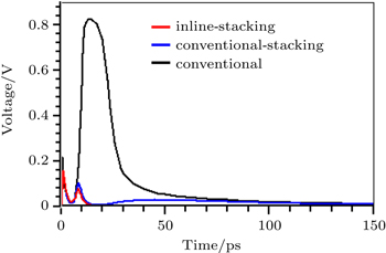
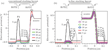
The potential variation can also help us to understand FBE in the stacking layout. As shown in Fig. 7(a), in the conventional stacking layout, the channel potential barrier of P2 is decreased greatly to about 0.06 V during ion strike, while the channel potential barrier of P1 is decreased to about 0.1 V slowly. Thus, source injection becomes possible, just like Fig. 5(b) shows. Because the channel potential barrier of P1 is almost twice that of P2, the source injection cannot bring about a propagating SET. Nevertheless, it is still a potential threat, and in in-line stacking layout, it is removed completely. As shown in Fig. 7(b), the channel potential barrier of P1 remains about 0.28 V, whether the channel potential barrier of P2 is decreased or not. Thus, almost no source injection occurs in in-line stacking layout, and the in-line stacking layout is more superior.

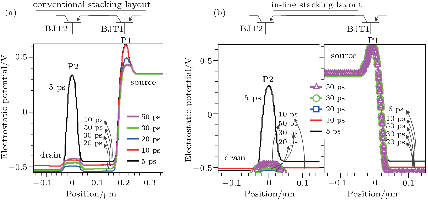
Fig. 7. With ion striking at the gate center of P2 with ion LET of 20 MeV·cm2/mg, 1D electrostatic potential variation with time for P1 and P2 (a) in conventional stacking layout, (b) in in-line stacking layout. The cut-point is at the depth of 10 nm, and the gate center of P2 and P1.
4.2. N-hit simulation

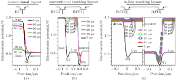
For N-hit simulations, as ion strikes at the gate center of NMOS (i.e., N0 and N2 in Fig. 1) with ion LET of 20 MeV·cm2/mg, the current transient curve is shown in Fig. 8, which is similar to that in P-hit simulations. As shown in Fig. 8, the drain current in the conventional layout is the largest and the peak is over 3 times larger than others, which also indicates that FBE can enhance charge collection greatly. As shown in Figs. 8(b) and 8(c), though charge collection at the drain is inevitable due to carrier drift/diffusion (the first peak in Fig. 8), its duration is so short that charge collection from carrier drift/diffusion cannot bring about propagating SET, and the source injection current is reduced greatly in the two stacking layouts, especially in the in-line stacking layout, it is almost cut down completely. Therefore, FBE is still the main cause of SET in FD-SOI NMOS, and stacking layout is beneficial for mitigation FBE in NMOS as well. Besides, in the in-line stacking layout, two transistors are separated by shallow trench isolation (STI), and then the charge deposited around a transistor cannot diffuse to another one. Thus, normal ion strike cannot disturb the channel potential of two transistors, and then FBE is mitigated in the in-line stacking layout completely. Therefore, the in-line stacking layout is more superior in mitigating single event sensitivity.

Fig. 8. With ion striking at the gate center of N0 or N2 (shown in Fig. 1) with ion LET of 20 MeV·cm2/mg, the drain and source current transient (a) in conventional layout, (b) in conventional stacking layout, and (c) in in-line stacking layout.

The potential variation with time is shown in Fig. 9. For transistor N0, ion strike at the gate center can cut down the channel potential barrier rapidly, as shown in Fig. 9(a), at 10 ps, the maximum channel potential rises from 0.32 V to 0.53 V, the increase is over 0.2 V and the channel potential barrier is reduced to about 0.04 V, so that the parasitic BJT is opened to activate the FBE. For the stacking layout, after ion strike, the channel potential barrier in transistor N2 is reduced greatly and fast, i.e., parasitic BJT2 is opened. However, the channel potential barrier in transistor N1 varies slowly. The channel potential barrier in N1 is always larger than about 0.95 V in the conventional stacking layout, while it is almost constant in the in-line stacking layout. That is, the channel potential of N1 is disturbed slightly in the conventional stacking layout, while it is not disturbed in the in-line stacking layout. Therefore, the in-line stacking layout is more superior in mitigating FBE.

Fig. 9. With ion striking at the gate center of N0 or N2 (shown in Fig. 1) with ion LET of 20 MeV·cm2/mg, 1D electrostatic potential variation with time (a) in conventional layout, (b) in conventional stacking layout, (c) in in-line stacking layout. The cut-point is at the depth of 10 nm, and the gate center of N0 or (N1 and N2).
5. Discussion
5.1. Angular simulation

Under normal ion strike, the in-line stacking layout is superior, for it can mitigate FBE completely. How about angular strike? As shown in Fig. 10, when changing ion incidence tilt from 0 to 90° with ion striking at the gate center, the single event responses of the two layouts are different. Theoretically, the two parasitic BJT should be opened to cause a SET at the drain. As shown in Table 1, TCAD simulation results indicate that the critical tilt to cause a SET is 77° and 84° respectively for conventional stacking PMOS layout and in-line stacking PMOS layout.

Fig. 10. Simulation setup for angular P-hit simulation. (a) Conventional layout, (b) in-line stacking layout.
Table 1.

Comparison of critical tilt for a SET generating in angular simulations.

.

In total, if the tilt is larger than the critical tilt in angular simulation, the two parasitic BJTs will be opened simultaneously, and then FBE occurs and large amount of charges are injected from source to cause a propagating SET. However, the critical tilt for IS layout is large enough to exceed 80°, the probability for a heavy-ion in aerospace to upset the transistor state in IS layout is small. Thus, we can conclude that the single event sensitivity of IS layout is still greatly superior over the conventional stacking layout.

5.2. The extension application to other logical gates

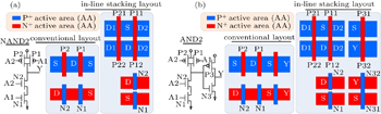
Since the in-line stacking technique is very effective for FBE mitigation, it can be applied into the hardening design of the standard cell library in FD-SOI technology. For those gates with stacking transistors, for example the NMOS transistors in NAND2 gate shown in Fig. 11, the IS layout technique can be used directly. However, for those transistors without stacking structure, for example, the PMOS transistors in NAND2 gate, they should be split into two tandem transistors severally, and then the IS layout technique can be used.

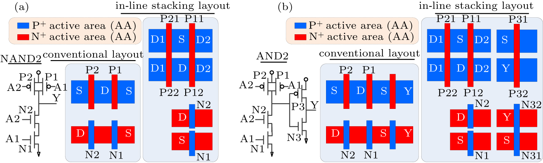
Fig. 11. (a) NAND2 gate and its conventional layout as well as the corresponding IS layout, (b) AND2 gate and its conventional layout as well as the corresponding IS layout.

As shown in Fig. 11, the implementation of IS layout needs to change their connection or even increase the space between some transistors with STI, thus, the area penalty of IS layout is inevitable. In Table 2, the area penalty of IS technique in several of the most common standard cells is listed. For INVX1 (inverter) gate, the area penalty for conventional stacking layout and IS layout is 1.33 times and 1.5 times respectively. In conventional stacking layout, the height of the cell remains constant, but the width of the cell will increase to 2N − 1 grid in general if the width of the conventional layout is N grid. Therefore, the area penalty of conventional stacking layout is 2 − 1/N times except for INVX1 gate, which is close to 2 as N is large enough. However, in IS layout, the height of the cells is increased 1.5 times, but its width is just increased about M grid if there are 2M transistors sharing their sources. Generally, for those two-stage gates, such as OR2X1 gate, M is 1. Therefore, the IS layout technique is still superior in area saving.

Table 2.

Comparison of several of the most common standard cell areas.

.
6. Conclusion

Based on 3D-TCAD numerical simulation, the effect of floating body effect on SET generation in FD-SOI technology is investigated. Whether for PMOS or NMOS, the main mechanism for SET generation is not carrier drift/diffusion but FBE, and mitigating FBE is the main approach to mitigate single event sensitivity. In this paper, two stacking layout designs are simulated as well. The simulation results indicate that the IS layout is superior over the conventional stacking layout in reducing single event sensitivity and saving area penalty. In particular, for normal strike simulations, the IS layout can mitigate FBE completely, which is exciting for having a hardening design in FD-SOI technology.

Reference
1Cannon E HReinhardt D DGordon M SMakowenskyj P S2004IEEE 04CH37533 42nd Annual International Reliability Physics Symposium, Phoenixp. 300
2Gasiot GRoche PFlatresse P2008IEEE CFP08RPS-CDR 46th Annual International Reliability Physics Symposium, Phoenixp. 192
3Heidel D FMarshall P WPellish J ARodbell K PLabel K ASchwank J RRauch S EHakey M CBerg M DCastaneda C MDodd P EFriendlich M RPhan A DSeidleck C MShaneyfelt M RXapsos M A 2009 IEEE Trans. Nucl. Sci. 56 3499
4Zhang KManzawa YKobayashi K2014IEEE Intl. Reliability Phys. Symp.SE.2.1
5Gouker PBrandt JWyatt PTyrrell BSoares AKnecht JKeast CMcMorrow DNarasimham BGadlage MBuhva B 2008 IEEE Trans. Nucl. Sci. 55 2854
6Cavrois V FPouget VMcMorrow DSchwank J RFel NEssely FFlores R SPaillet PGaillardin MKobayashi DMelinger J SBuhamel ODodd P EShaneyfelt M R 2008 IEEE Trans. Nucl. Sci. 55 2842
7Moen K APhillips S DWilcox E PXCressler J DNayfeh HSutton A KWarner J HBuchner S PMcMorrow DVizkelethy GDodd P 2010 IEEE Trans. Nucl. Sci. 57 3366
8Gadlage M JAhlbin J RRamachandran VGouker PDinkins C ABhuva B LNarasimham BSchrimpf R DMcCurdy M WAllies M LReed R AMendenhall M HMassengill L WShuler R LMcMorrow D 2009 IEEE Trans. Nucl. Sci. 56 3115
9Dodd P EMassengill L W 2003 IEEE Trans. Nucl. Sci. 50 583
10Schwank J RCavrois V FShaneyfelt M RPaillet PDodd P E 2003 IEEE Trans. Nucl. Sci. 50 522
11Cavrois V FPaillet PGaillardin MLambert DBaggio JSchwank J RVizkelethy GShaneyfelt M RKirose KBlackmore E WFaynot OJahan CTosti L 2006 IEEE Trans. Nucl. Sci. 53 3242
12Colladant TFlament OHoir A LCavrois V FD’Hose CduPortdePontcharra J 2002 IEEE Trans. Nucl. Sci. 49 2957
13Hirose KSaito HKuroda YIshii SFukuoka YTakahashi D 2002 IEEE Trans. Nucl. Sci. 49 2965
14Hirose KSaito HKuroda YIshii STakahashi DYamamoto K 2004 IEEE Trans. Nucl. Sci. 51 3349
15Huang PChen SLiang ZChen JHu CHe Y 2014 Chin. Sci. Bull. 59 2850
16Huang PChen SChen JLiang BLiu B 2014 IEEE Trans. Dev. Mat. Rel. 14 849
17Chen J JChen S MLiang BDeng K F 2012 Chin. Phys. B 21 016103
18Chen S MChen J J 2012 Chin. Phys. B 21 016104
19Chen J JChi Y QLiang B 2015 Chin. Phys. B 24 016102
20Huang PChen SChen JLiang BChi Y 2015 IEEE Trans. Nucl. Sci. 62 3330