Spoof surface plasmon-based bandpass filter with extremely wide upper stopband
[Liu Xiaoyong1, 2, Zhu Lei2, †,  , Feng Yijun1, ‡, ]
, Feng Yijun1, ‡, ]
|
|


† Corresponding author. E-mail:
‡ Corresponding author. E-mail:
Project supported by the Key Grant Project of Ministry of Education of China (Grant No. 313029), the FDCT Research Grant from Macao Science and Technology Development Fund, China (Grant No. 051/2014/A1), and the Multi-Year Research Grant from University of Macau, Macau SAR, China (Grant No. MYRG2014-00079-FST).
We investigate the guiding modes of spoof surface plasmon polaritons (SPPs) on a symmetric ultra-thin plasmonic structure. From the analysis, we deduce the operating frequency region of the single-mode propagation. Based on this property, a spoof SPPs lowpass filter is then constituted in the microwave frequency. By introducing a transmission zero at the lower frequency band using a pair of stepped-impedance stubs, a wide passband filter is further realized. The proposed filter is fed by a transducer composed of a microstrip line with a flaring ground. The simulated results show that the presented filter has an extremely wide upper stopband in addition to excellent passband filtering characteristics such as low loss, wide band, and high square ratio. A prototype passband filter is also fabricated to validate the predicted performances. The proposed spoof-SPPs filter is believed to be very promising for other surface waveguide components in microwave and terahertz bands.
Surface plasmon polaritons (SPPs) are the surface electromagnetic (EM) waves propagating along a dielectric–metal interface at the optical frequencies.[1] Owing to the unique properties of guiding and localizing electromagnetic (EM) waves into sub-wavelength scales, the SPPs have attracted increasing attention in the past decade.[2,3] The intrinsic properties associated with the SPPs have enabled potential applications of designing highly integrated circuits and devices in the areas of optoelectronics, material science, and biosensing. There is also increased interest to extend the unique properties of the SPPs to lower frequencies for the exploration of various integrated circuits and devices in the terahertz (THz) and microwave regimes. However, as a metal resembles a perfect electric conductor (PEC) in these low frequency regimes, the SPPs cannot be supported on smooth metal surfaces.
Recently, plenty of works have demonstrated that the highly confined surface EM waves, named spoof SPPs or designer SPPs, could be supported by plasmonic metamaterials, which usually consist of a textured metal surface with sub-wavelength scaled grooves or dimples.[4–12] The surface plasmon frequency and the SPP-like dispersion property of the spoof SPPs could be scaled down to the THz or microwave region by using these plasmonic metamaterials. However, all these plasmonic metamaterials with non-planar geometry primarily rely on a three-dimensional (3D) structure of the sub-wavelength scaled geometry on metal surfaces, making them inconvenient to be fabricated and integrated with other existing THz or microwave circuitries. More recently, an ultra-thin plasmonic metamaterial has been proposed to support spoof SPPs.[13–16] Due to its flexible and planar property, such ultra-thin plasmonic metamaterial paves a way for developing versatile surface wave integrated devices or circuits at lower bands, especially at the THz region.
Spoof SPPs based devices, such as ultra-thin surface plasmonic bandpass filters, were also reported,[17–19] which show excellent filtering characteristics such as low loss, wide band, and high square ratio. However, the upper stopband of the reported ultra-wideband filter is very narrow,[17] which is also exhibited in other ultra-wideband microstrip line filter designs.[20] Thereafter, more effort is still needed to design a bandpass filter with an extremely wide upper stopband that is highly demanded in practical applications for effective suppression of the undesired noise signal.
In this paper, by detailed study of the condition or operating frequency region of the single mode propagation of spoof SPPs on a symmetric ultra-thin plasmonic structure, we propose a spoof SPPs based wide passband filter with an extremely wide upper stopband. It is designed by combining the cut-off of the spoof SPPs with a transmission zero created through a pair of shunt stepped-impedance stubs at the lower frequency band. A flaring ground is also employed in the connecting microstrip line to feed the proposed filter. Both simulation and measurement results on S-parameters have demonstrated the emergence of an extremely wide upper stopband above the desired wide passband.
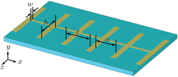
The symmetric spoof SPPs structure is composed of a thin metal strip on the top of a dielectric substrate with a thickness of 0.813 mm, relative dielectric constant of 3.55, and loss tangent of 0.003. Herein, the two sides of the metallic strip are symmetrically corrugated by a one-dimensional array of grooves with depth h, width a, lattices constant d, and central line width w, as schematically illustrated in Fig.


 | Fig. 1. Geometry of an ultra-thin symmetric spoof SPPs waveguide on a dielectric substrate. |
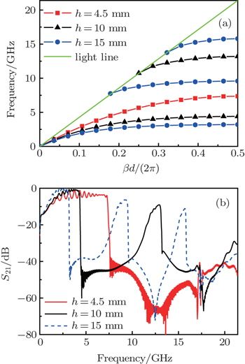
 | Fig. 2. (a) Dispersion relation of spoof SPPs for different groove depths h. The parameters d, a, and w are set as 7.0 mm, 6.0 mm, and 0.3 mm, respectively. (b) The corresponding transmission spectra. |
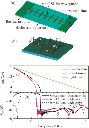
In order to achieve an efficient single-mode transmission, we adopt the microstrip line with a flaring ground as a bridge or transition from the SMA connectors to the spoof SPPs waveguide, as shown in Fig.
 | Fig. 3. (a) Schematic diagram of the symmetric spoof SPPs structure with input and output microstrip line sections. (b) Schematic diagram of a shunt stepped-impedance resonator. (c) Calculated dispersion curve. (d) Simulated results of a spoof-SPPs based lowpass filter and the bandpass filter with stepped-impedance resonators added. |
Based on the previous transmission spectrum of the spoof SPPs, a wide bandpass filter with an extremely wide upper stopband can be further obtained by introducing a transmission zero at the low frequency band. In our study, a shunt stepped-impedance resonator is installed in the section of the microstrip line to acquire the transmission zero,[22] which consists of two impedance sections as z1 and z2 with lengths L1 and L2, respectively, as shown in Fig.

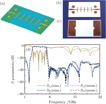
According to the previous analysis, we propose a bandpass filter structure as shown in Fig.
 | Fig. 4. (a) Schematic diagram of the proposed bandpass filter structure. The front (b) and the back (c) side photographs of the fabricated prototype filter. (d) The simulated and measured S parameters of the filter. |
Next, we fabricate a prototype sample and conduct microwave experiments to test the designed bandpass filter. A sample of the proposed filter is fabricated on a commercial print circuit board (PCB) dielectric substrate (Rogers 4003C, 0.813 mm), as shown in Figs.
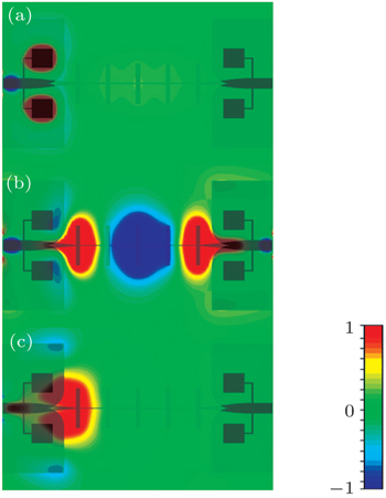
To get an insight into the filtering characteristics, the simulated y component of the electric field is plotted in Fig.
 | Fig. 5. The simulated electric field Ey distributions on the surface of the filter at the frequencies of (a) 2.28 GHz, (b) 5 GHz, and (c) 9 GHz, respectively. |
We have extensively analyzed the guiding modes on a symmetric spoof SPPs structure. It shows that the mode number is mainly determined by the ratio between the groove depth and the lattice constant. Single-mode propagation may be supported by choosing a suitable ratio of these two parameters. Based on this property, a wide passband filter with a wide upper stopband has been designed at the microwave frequency range by introducing a transmission zero at the lower frequency band. To verify the predicted performance, we fabricated a prototype filter. The measured results of the filter validate the emergence of an extremely wide upper stopband above the desired passband. We believe that the proposed spoof SPPs filter is very promising for the exploration of other surface waveguide components or systems in both the microwave and terahertz bands.
| 1 | |
| 2 | |
| 3 | |
| 4 | |
| 5 | |
| 6 | |
| 7 | |
| 8 | |
| 9 | |
| 10 | |
| 11 | |
| 12 | |
| 13 | |
| 14 | |
| 15 | |
| 16 | |
| 17 | |
| 18 | |
| 19 | |
| 20 | |
| 21 | |
| 22 |