


Room temperature NO2 gas sensing of Au-loaded tungsten oxide nanowires/porous silicon hybrid structure
Cite this Article
Wang Deng-Feng, Liang Ji-Ran, Li Chang-Qing, Yan Wen-Jun, Hu Ming. Room temperature NO2 gas sensing of Au-loaded tungsten oxide nanowires/porous silicon hybrid structure. Chinese Physics B, 2016, 25(2): 028102 
Permissions
Room temperature NO2 gas sensing of Au-loaded tungsten oxide nanowires/porous silicon hybrid structure
† Corresponding author. E-mail:
Project supported by the National Natural Science Foundation of China (Grant Nos. 61274074 and 61271070) and the Key Research Program of Application Foundation and Advanced Technology of Tianjin, China (Grant No. 11JCZDJC15300).
Abstract
Abstract
In this work, we report an enhanced nitrogen dioxide (NO2) gas sensor based on tungsten oxide (WO3) nanowires/porous silicon (PS) decorated with gold (Au) nanoparticles. Au-loaded WO3 nanowires with diameters of 10 nm–25 nm and lengths of 300 nm–500 nm are fabricated by the sputtering method on a porous silicon substrate. The high-resolution transmission electron microscopy (HRTEM) micrographs show that Au nanoparticles are uniformly distributed on the surfaces of WO3 nanowires. The effect of the Au nanoparticles on the NO2-sensing performance of WO3 nanowires/porous silicon is investigated over a low concentration range of 0.2 ppm–5 ppm of NO2 at room temperature (25 °C). It is found that the 10-Å Au-loaded WO3 nanowires/porous silicon-based sensor possesses the highest gas response characteristic. The underlying mechanism of the enhanced sensing properties of the Au-loaded WO3 nanowires/porous silicon is also discussed.
1. Introduction
Nitrogen dioxide (NO2), often produced in coal, coal oil or natural gas manufacturing, is a toxic gas that harms the environment and human health even at extremely low concentrations and a sub-ppm level. When the concentration of NO2 is higher than 20 ppm, it is dangerous to the human body and may cause death. Reliable NO2 sensor with high sensitivity, selectivity and low energy consumption is highly demanded for environmental safety and industrial control. In recent years, one-dimensional metal oxide nanocomposites have attracted enormous attention due to their unique electronic properties, flexible structures and excellent adsorptions. Many recent studies have shown that the important sensing parameters of one-dimensional metal oxide sensors can be improved by making them composite ones (e.g., dissimilar metal oxide,[1–6] organics,[7] and other semiconductors[8–11]), which opens a new door to realize smart sensor systems based on nanostructured materials in the NO2 gas sensing industry.[12–15]
Tungsten oxide (WO3), a typical n-type metal oxide semiconductor with a relatively large indirect band gap of 2.8 eV exhibits promising application potentials in catalytic/photocatalytic processing, humidity and temperature sensors, biosensors and photonic crystals[16–19] in comparison with their diverse crystal types and also has unique electrochromic, optochromic and gaschromic properties. In the research of gas sensor applications, the gas sensitivity of WO3 heavily depends on film parameters, such as composition, morphology (e.g., grain size), nanostructure and microstructure (e.g., porosity, surface-to-volume ratio).[20,21] Since one-dimensional tungsten oxides, including nanowires and nanorods, exhibit high crystallinities and large surface-to-volume ratios[22–24] compared with their bulk materials, extensive efforts have been made synthesize the tungsten oxide nanostructures and assembled ordered superstructures for detecting NO2 gas. Porous silicon (PS), fabricated simply by electrochemical etching of silicon resulting in periodically arranged arrays of pores, has been widely used as a scaffold to synthesize nanowires and nanotubes.[25–28] It is facile to tune pore diameters and pore spacing by adjusting parameters such as the type of electrolyte, the PH, and the applied voltage. Therefore, the composites of one-dimensional nanomaterials/PS may have enhancing effects.
The functional properties of the metal oxide-based gas sensors can be improved not only by tailoring the crystal size of metal oxides but also by adding noble metal (Pt, Pd, Ag, etc.).[29–32] It was observed that the surface modification of nanocrystalline metal oxide by noble metal sensitizers reduced the operating temperatures appreciably and improved the sensing properties towards target gas species. Liu et al.[33] reported a shape-controlled synthesis of Pd nanocubes on WO3 nanoplates by a solvothermal method, which presented a high and fast response at room temperature. Liu et al.[34] also prepared a Pt-WO3 sensor which exhibited a fast response and recovery as well as a high sensitivity compared with the undecorated sensor. Many studies have been performed to fabricate metal oxide semiconductor materials and to optimize their detection capability and optimum working conditions. Also, though WO3 and Au are investigated intensively in the literature, not many studies of their properties after mixing and subsequent annealing have been conducted. What we have done for the first time is to successfully synthesize the Au-loaded WO3 nanowires on PS substrates.
In this paper, we report a novel synthesis of Au-loaded WO3 nanowires/PS composite, which presents good sensitivity and selectivity. In addition, the NO2 sensing characteristics of this composite are compared with those of unloaded WO3 nanowires/PS. The Au-loaded WO3 nanowires/PS composite exhibiting an enhanced NO2 response may be attributed to the excellent dispersion of Au nanoparticles on WO3 nanowires having a very large effective surface area, leading to highly effective spillover of molecular nitrogen dioxide through Au nanoparticles onto the WO3 nanowires surface. More importantly, this work suggests that seeking methods to form composite structures between noble metal and WO3 nanowires/PS is a promising strategy to improve the performance of gas-sensing.
2. Experiment
The Au-loaded WO3 nanowires/PS composites were prepared by the following process. First, the PS substrate with large pore size (1 μm–1.5 μm) was prepared by an electrochemical etching method in a Teflon double-cell configuration, which was described in detail in our previous work.[35] Silicon substrate was designed to be 22 mm × 9 mm after cutting from a p-type (100)-orientation monocrystalline silicon wafer with a resistivity of 10 Ω·cm–15 Ω ·cm. The wafer was placed in an electrolyte solution, which was composed of a 1:2 volume mixture of 40-wt% hydrofluoric acid and 99.5-wt% N,N-dimethyl formamide (DMF). The etching current density and etching time were 100 mA·cm−2 and 8 min, respectively.[36] Before the etching process, the Si substrate was cleaned necessarily and immersed in hydrofluoric acid to remove the oxide layer. The etching process was carried out at room temperature (RT). After etching, all PS samples were rinsed with ethanol and dried in air. In order to obtain WO3 nanowires/PS composite, a metallic tungsten film with a thickness of 150 nm was pre-deposited on the PS substrate by DC magnetron sputtering. Subsequently, the sputtered PS substrates were placed in the hot zone of a horizontal tube furnace. After the quartz tube was pumped to a vacuum of 5 × 10⁻² Torr (1 = 1.33322 × 10² Pa), a mixture of argon and oxygen was introduced at rates of 80 sccm and 0.5 sccm, respectively. Then the tube furnace temperature increased gradually from room temperature to 700 °C and was maintained at this temperature for 1 h. The schematic diagram for synthesizing the WO3 nanowires/PS composite is shown in Fig.
The surface morphologies of the samples were investigated by field emission scanning electron microscopy (FESEM, Hitachi S4800). The phase structures of unloaded and Au-loaded WO3 nanowires were examined by x-ray diffraction (XRD, RIGAKU D/MAX 2500V/PC, Cu Kα radiation). High-resolution transmission electron microscopy (HRTEM, Tecnai G2 F20) and energy dispersive x-ray spectroscopy (EDXS) were also used to confirm the presence of Au nanoparticles on WO3 nanowires.
 | Fig. 1. Schematic diagram for synthesizing WO3 nanowires/porous silicon composite. |
The gas sensing properties of the unloaded and Au-loaded WO3 nanowires/porous silicon were measured in a home-made testing system consisting of a sealed 30-L test chamber, a heating plate with an adjustment range of temperature from RT to 300 °C, a professional digital multimeter (NUI-T UT70D), a data acquisition PC, and a stirring mini-fan to promote the diffusion of the detected gas. Pure target gas was injected into the test chamber directly to obtain the desired concentration. The ambient relative humidity is about 35% during the entire measurement. The resistance change of the sensors during the whole measurement process was continuously monitored by the multimeter.[37] The gas sensing response (S) is given by S = Rg/Ra, where Rg and Ra are the resistances of the samples in oxidizing gas and air, respectively.
3. Results and discussion
3.1. Structure characterization
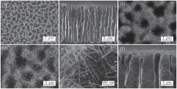
Figures
 | Fig. 2. SEM images of (a) plan view and (b) cross section view of the porous silicon, (c) unloaded WO3 nanowires/porous silicon, (d) low magnification, (e) high magnification, and (f) corresponding cross-sectional SEM image of Au-loaded WO3 nanowires. |
The diffraction spectra of unloaded WO3 nanowires and Au-loaded WO3 nanowires with different amounts of Au content are presented in Fig.
Figure
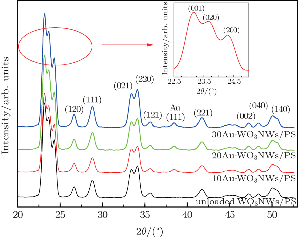 | Fig. 3. XRD patterns of Au-loaded WO3 nanowires. |
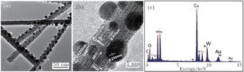
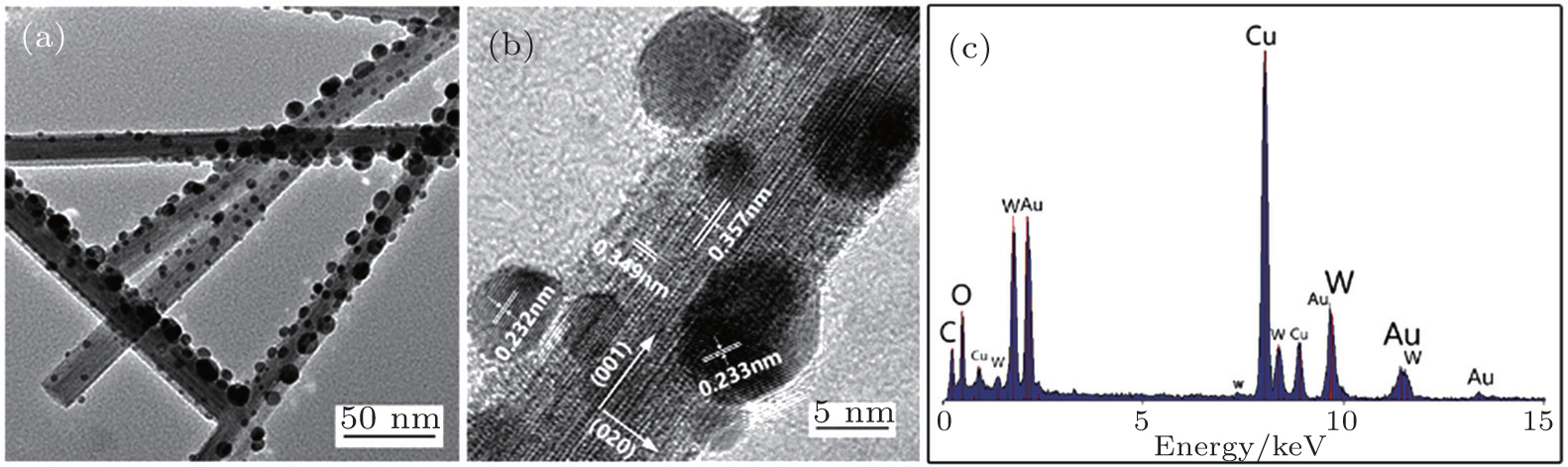 | Fig. 4. (a) TEM and (b) HRTEM images and (c) EDS spectrum of obtained samples. |
3.2. Gas sensing properties of NO2
Figure
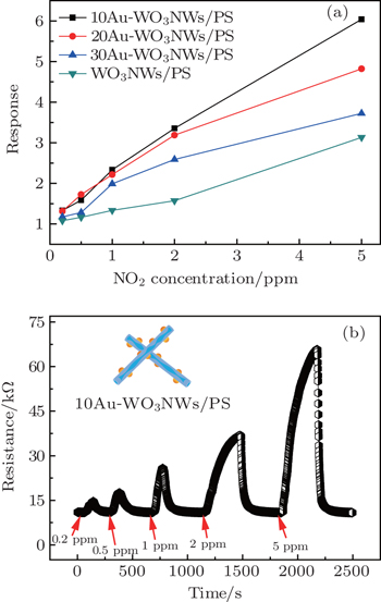
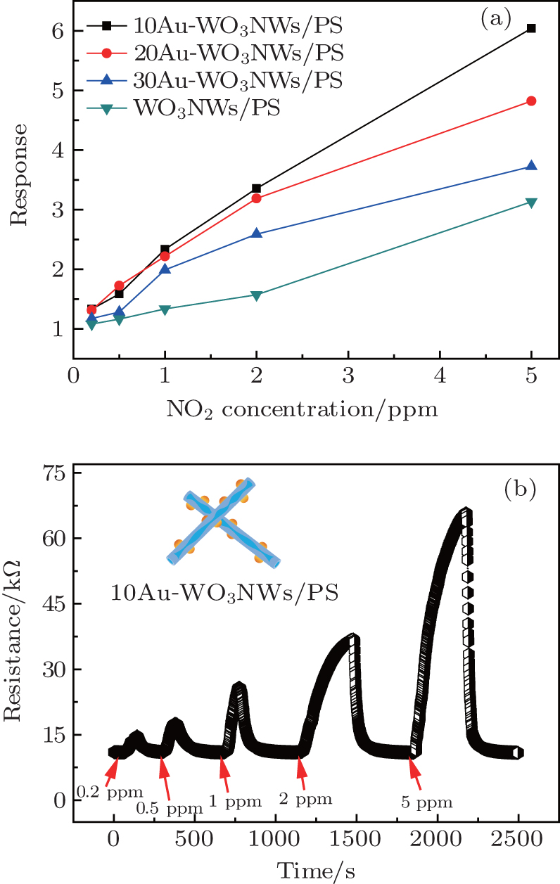 | Fig. 5. (a) Sensing performances of unloaded and loaded WO3NWs/PS to different concentrations of NO2 at room temperature; (b) dynamic response of 10Au-WO3NWs/PS. |
3.3. NO2 sensing mechanism
As has been reported, WO3 is a representative n-type semiconductor with a surface-controlled sensing mechanism. The change of resistance is largely dependent on the amount and the species of chemisorbed oxygen on the surface. Figures
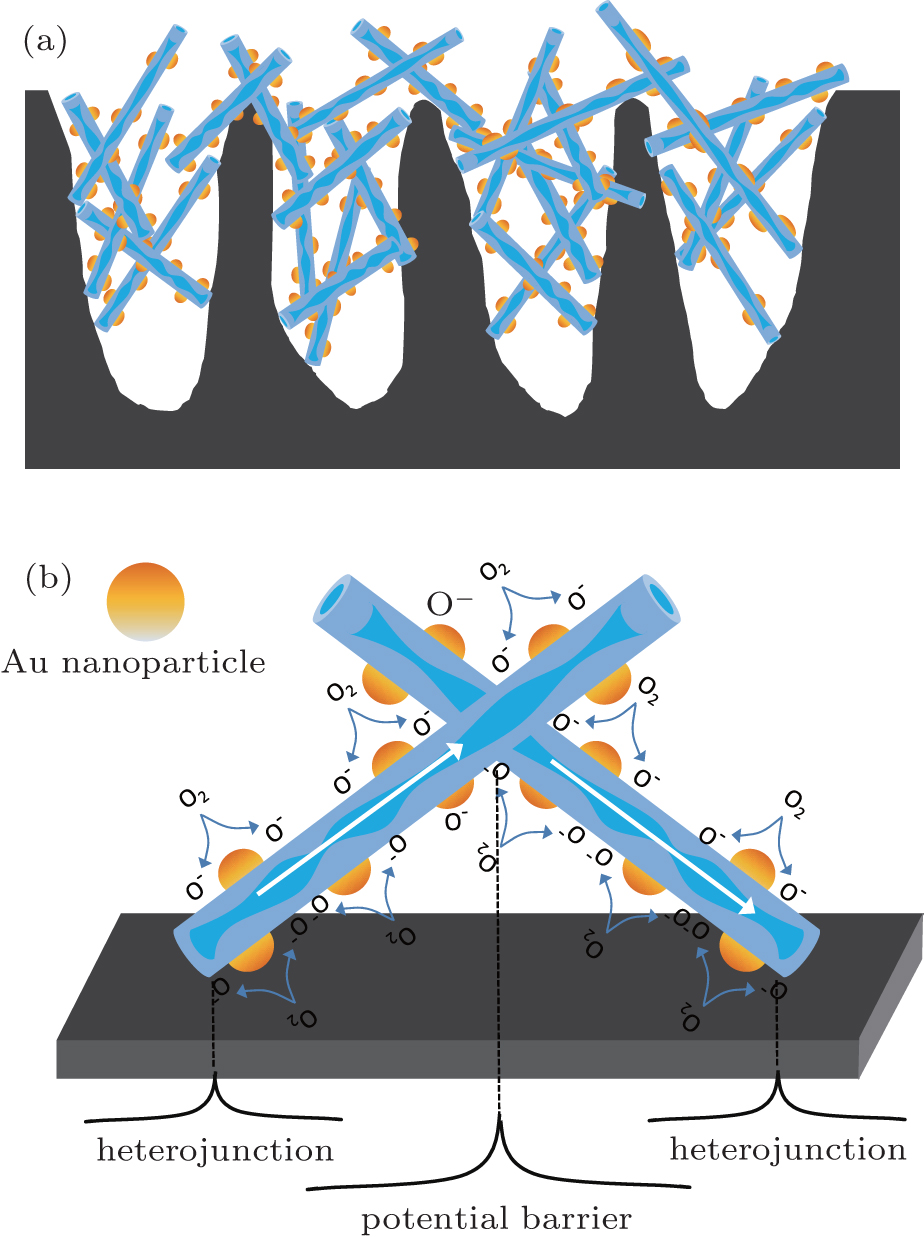 | Fig. 6. (a) Schematic illustration of a network of Au-loaded WO3 nanowires/porous silicon composite sensor and (b) the gas sensing mechanism. |
The highly distributed Au nanoparticles on the surfaces of WO3 nanowires facilitate the ion sorption of the oxygen molecules (


Electrons in the conduction band can be easily captured by the oxygen species. Therefore, an electron depletion layer is formed on the WO3 nanowire surface. When NO2 gas is introduced into the experimental cavity, it is adsorbed directly on the surface of the WO3 nanowire and reacts with the adsorbed O− (ads) by the following reactions:[41]


Both reactions take free electrons from the conduction band of WO3 resulting in a wider electron depletion layer, which is supposed to narrow the conducting channel of WO3 nanowire thereby increasing the nanowire surface resistance. Furthermore, the heterojunction formed at the interface between WO3 nanowire and porous silicon should also be taken into account.[42] The heterojunction prompts the electrons to flow from the porous silicon with a low work function to WO3 with a high work function until their Fermi levels equalize, which creates an electron depletion layer or potential barrier at the interface and bends the energy band. When NO2 gas is adsorbed, the electrons associated with these charged species are drawn from the conduction band. As a result, the initial depletion layer further extends to increase the potential barrier height of the heterojunction.
The notable phenomenon in Fig.
4. Selectivity
Figure
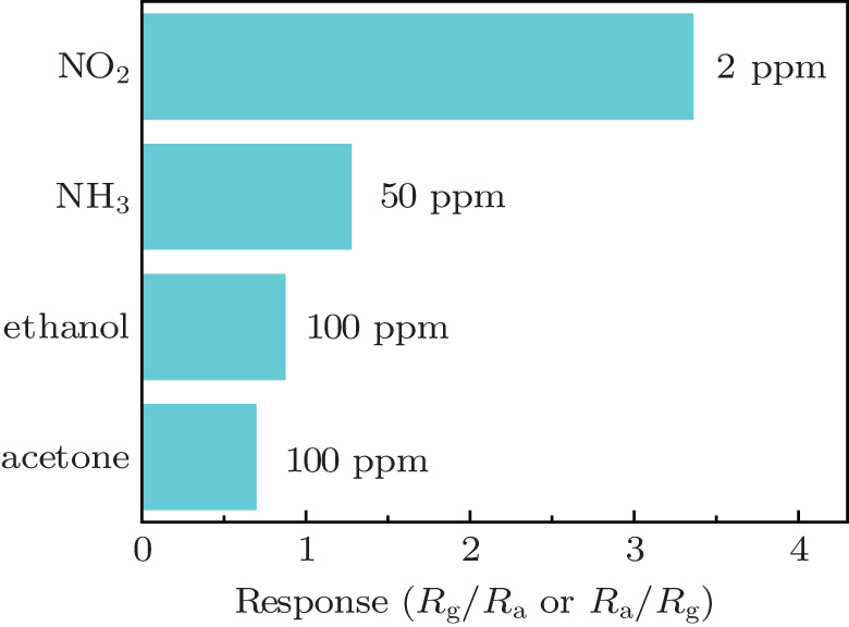 | Fig. 7. Selectivities of Au-WO3NWs/PS at room temperature. |
5. Conclusions
In this work Au loaded WO3 nanowires/PS composites with Au layer thickness values ranging from 10 Å to 30 Å, are prepared by the sputtering method. The structures and morphologies of the WO3 nanowires are investigated by using XRD, FE-SEM, and TEM. The XRD results show that the WO3 nanowires present a well orthorhombic system after the thermal treatment at 400 °C for 1 h. SEM and TEM analyses show that Au nanoparticles disperse evenly on the surfaces of the prepared products. The 10Au-WO3NWs/PS sensor shows a high response (3.357) and good selectivity to 2-ppm NO2 at room temperature. Therefore the sensor based on WO3 with a proper Au loading demonstrates a promising process in the field of gas detection.
Reference
| 1 | |
| 2 | |
| 3 | |
| 4 | |
| 5 | |
| 6 | |
| 7 | |
| 8 | |
| 9 | |
| 10 | |
| 11 | |
| 12 | |
| 13 | |
| 14 | |
| 15 | |
| 16 | |
| 17 | |
| 18 | |
| 19 | |
| 20 | |
| 21 | |
| 22 | |
| 23 | |
| 24 | |
| 25 | |
| 26 | |
| 27 | |
| 28 | |
| 29 | |
| 30 | |
| 31 | |
| 32 | |
| 33 | |
| 34 | |
| 35 | |
| 36 | |
| 37 | |
| 38 | |
| 39 | |
| 40 | |
| 41 | |
| 42 |