Fan Ji-Bin, Ding Xiao-Fu, Liu Hong-Xia, Xie Peng-Fei, Zhang Yuan-Tao, Liao Qing-Liang. Improvement in electrical properties of high-κ film on Ge substrate by an improved stress relieved pre-oxide method. Chinese Physics B, 2016, 25(2): 027702
Permissions
Improvement in electrical properties of high-κ film on Ge substrate by an improved stress relieved pre-oxide method
Fan Ji-Bin1, 2, †, , Ding Xiao-Fu1, Liu Hong-Xia2, Xie Peng-Fei1, Zhang Yuan-Tao1, Liao Qing-Liang1
School of Materials Science and Engineering, Chang'an University, Xi'an 710061, China
School of Microelectronics, Key Laboratory of Wide Band-Gap Semiconductor Materials and Devices, Xidian University, Xi'an 710071, China
† Corresponding author. E-mail: jbfan@chd.edu.cn
Abstract
Abstract
High-κ/Ge gate stack has recently attracted a great deal of attention as a potential candidate to replace planar silicon transistors for sub-22 generation. However, the desorption and volatilization of GeO hamper the development of Ge-based devices. To cope with this challenge, various techniques have been proposed to improve the high-κ/Ge interface. However, these techniques have not been developed perfectly yet to control the interface. Therefore, in this paper, we propose an improved stress relieved pre-oxide (SRPO) method to improve the thermodynamic stability of the high-κ/Ge interface. The x-ray photoelectron spectroscopy (XPS) and atomic force microscopy (AFM) results indicate that the GeO volatilization of the high-κ/Ge gate stack is efficiently suppressed after 500 °C annealing, and the electrical characteristics are greatly improved.
Recently, the high-κ/Ge gate stack with high-mobility substrates has been explored in order to continue to scale down the ultra-low power and high speed microelectronic devices.[1–3] One of the main concerns about high-κ/Ge gate stack devices is that Ge–O bonds inevitably exist at the interface between Ge and high-κ films and its volatilization occurs even below 500 °C, which is required for source/drain activation for the complementary metal–oxide semiconductor (CMOS) fabrication process.[4,5] Volatilization of GeO out of the air will generate a huge number of defects and traps in the high-κ film after GeO desorption and volatilization.[6,7] It tends to deteriorate the interface and high-κ film quality, leads to the gate leakage current largely increasing, mobility and reliabilities degrading obviously.[8,9] The mechanism of the GeO desorption is proposed to be that the interface oxygen vacancies generated at the GeO2/Ge interface diffuse into the GeO2 surface region.[10] Thus annealing the high-κ/Ge gate stacks without GeO desorption is the key process to realize a high-quality interface and high-κ film. To cope with this challenge, various techniques have been proposed to passivate the high-κ/Ge interface such as ultrathin Si or SiO2 capping layers,[11,12] GeOxNy passivation layer,[13] and high-quality GeO2 interfacial layers formed by plasma oxidation or ozone oxidation.[14–16] However, these techniques have not been developed perfectly yet to control the interface. Furthermore, some passivation layers have relatively low dielectric constants and may not enable scaling to low-EOT devices. Recently, a stress relieved pre-oxide (SRPO) treatment method is reported to improve the Si-based device characteristic and reduce the density of interfacial defects generated during the oxidation process.[17] Thus, in this paper, an improved SRPO treatment is investigated to improve the high-κ/Ge gate stack interface. The experimental results indicate that the improved SRPO treatment can suppress the GeO volatilization and improve the C–V characteristics of high-κ/Ge.
2. Experiment
In Ref. [17], an SRPO treatment using H2O2 solution to form a 7.5-Å chemical oxidized SiO2 layer on Si and then an annealing treatment was performed for stress relief. Owing to the fact that GeO2 is hydrolysable in H2O, the SRPO treatment is improved in this work. Before the deposition, the p-type (100) Ge wafers each with a resistivity of 0.3 Ω·cm are dipped in dilute HF (hydrofluoric acid: deionized water = 1:500) to remove the Ge oxide. Then, in-situ oxidation of the Ge surface in the UV/ozone ProCleaner plus system is carried out to grow 1.5-nm GeO2. After that, these films are annealed in ozone/O2 mixed gas at 400 °C for 120 s and then cleaned by dilute HF to keep 1.5-nm GeO2. Finally, Ge substrates cleaned by the standard RCA method each have 1.5-nm GeO2 and these Ge substrates are immediately placed into the ALD chamber to deposited 4-nm HfO2 films. They are denoted as sample A and sample B, respectively. After the samples A and B annealed in the nitrogen at 500 °C for 60 s, the XPS measurements are carried out by using a Thermo Scientific K-alpha system. Electrical measurements are carried out using a Keithley 590 CV meter and a Keithley 4200-SCS system after the Al electrode has been fabricated by depositing 200-nm aluminum using electron-beam evaporation.
3. Results and discussion
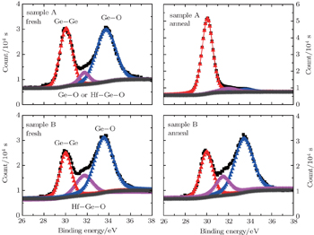
Figure 1 shows the XPS core-level spectra of Ge3d for HfO2 films on Ge substrates after annealing. The core level energies are obtained by curve fitting accurately measured binding energy of the peak, and the XPS spectrum is referred to the substrate Ge3d peak at a binding energy of 30.0 eV. We can see that the different changes are observed for sample A and sample B after annealing as shown in Fig. 1. For the fresh sample A, the Ge3d peak can be fitted with three peaks, which are located at the binding energies of 30.0 eV, 31.71 eV, and 33.65 eV, respectively. They are attributed to the Ge substrate, GeOx or HfGeO, GeO2, respectively.[18] After annealing, the peak intensities of GeO2 and GeOx or HfGeO peaks decrease significantly. It may be explained by the GeO volatilization caused by the GeO2/Ge interface reaction through the GeO2 + Ge → 2GeO (↑).[10] The GeO2 and Ge suboxide are consumed by the reaction of the GeO generation. Therefore, we conclude that the peak located at the binding energy of 31.71 eV should be more like Ge suboxide instead of HfGeOx.[8] For the fresh sample B, the Ge3d peak can also be fitted with three peaks, which are located at the binding energies of 30.0 eV, 31.56 eV, and 33.52 eV. They are attributed to the Ge substrate, HfGeOx or GeOx, GeO2, respectively.[18] After annealing, negligible peak change is observed for sample B, which indicates that the GeO generation is suppressed. The results show that the improved SRPO treatment provides high Ge4+ density and hafnium germinate is formed after deposition which works as an oxygen diffusion barrier and suppresses the GeO volatilization after annealing. However, for the samples with no SRPO treatment, deficient hafnium germinate mixed with the germanium suboxide is formed after deposition, which cannot work as an efficient oxygen diffusion barrier, the reaction of the GeO generation occurs and Ge oxide is consumed after annealing.
Fig. 1. The XPS core-level spectra of the Ge3d for HfO2 deposited on the Ge substrate (sample A) and Ge substrate after an improved SRPO treatment (sample B). Curve fitting is used to ensure high accuracy binding energy of the peak.
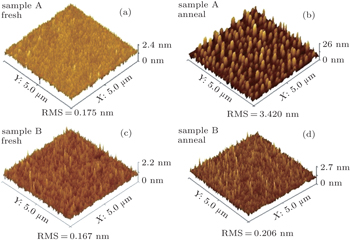
Since the fast desorption of GeO can form the thin film, the surface becomes rougher and rougher after GeO volatilization. The roughness of the surface can characterize the GeO volatilization intuitively as shown in Fig. 2. The root mean square (RMS) roughness of sample A increases sharply from 0.175 nm to 3.420 nm after annealing, whereas that of sample B only increases from 0.167 nm to 0.206 nm. The desorption of GeO may occur in a uniform or nonuniform model for the high-k/Ge system, and finally results in the formation and growth of the voids.[11] As a result, the RMS value of sample A increases nearly 20 times after annealing. These results suggest that the HfO2/Ge gate stack treated with an improved SRPO method can efficiently avoid destructing the GeO volatilization after annealing, which is consistent with the XPS spectra.
Fig. 2. AFM surface images of sample A and sample B before and after annealing.
Figure 3 shows the C–V curves of HfO2 films grown on Ge substrates before and after annealing (f = 100 kHz). The gate voltage (VG) is swept from accumulation to inversion and then reversely, i.e., from inversion to accumulation. Accumulation capacitance in the C–V curve of sample A decreases sharply. It can be explained by the increasing of the leakage current density due to the fact that the volatilization of GeO generates a great leakage channel and deteriorates the characteristics of the gate stack films. Compared with the RCA cleaned Ge substrate, the HfO2 deposited on the Ge substrate treated by the SRPO method presents a better electrical characteristic because the improved SRPO treatment reduces the GeO volatilization at the interfacial layer.
Fig. 3.C–V curves of different pre-treated HfO2/Ge structures (f = 100 kHz).
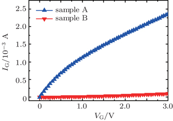
Figure 4 shows the I–V curves of HfO2 film grown on Ge substrates. As shown in Fig. 4, for the HfO2 film grown on the RCA-cleaned Ge substrate, the leakage current is 2.36×10⁻³ A at the bias gate voltage 3 V, whereas the leakage current is 9.90×10⁻⁵ A at the bias gate voltage 3 V for the HfO2 film grown on the Ge substrate processed by SRPO. The results indicate that the improved SRPO treatment suppresses the GeO volatilization and improves the interfacial characteristics of the HfO2/Ge structure during annealing, which is of benefit to decreasing the gate leakage current. It is consistent with the C–V testing result.
Fig. 4.I–V curves of different pre-treated HfO2/Ge structures.
4. Conclusions
In this work, the electrical properties of high-κ film on Ge can be substantially improved by an improved SRPO pretreatment after annealing. The XPS results indicate that GeO volatilization occurs obviously for non-SRPO treated HfO2/Ge samples after annealing, whereas the improved SRPO treated samples show that the GeO volatilization is suppressed due to the fact that an efficient Hf germanate oxygen diffusion barrier is formed and shows a small RMS variation. The electrical measurement results indicate that the improved SRPO treated HfO2/Ge gate MOS structure presents a good C–V characteristic and the gate current decreases significantly compared with non-SRPO treated samples.


 , Ding Xiao-Fu1, Liu Hong-Xia2, Xie Peng-Fei1, Zhang Yuan-Tao1, Liao Qing-Liang1]