Wang Yu-Ru, Liu Yi-He, Lin Zhao-Jiang, Fang Dong, Li Cheng-Zhou, Qiao Ming, Zhang Bo. Modeling of a triple reduced surface field silicon-on-insulator lateral double-diffused metal–oxide–semiconductor field-effect transistor with low on-state resistance. Chinese Physics B, 2016, 25(2): 027305
Permissions
Modeling of a triple reduced surface field silicon-on-insulator lateral double-diffused metal–oxide–semiconductor field-effect transistor with low on-state resistance
Wang Yu-Ru1, Liu Yi-He1, Lin Zhao-Jiang1, Fang Dong1, Li Cheng-Zhou1, Qiao Ming1, 2, †, , Zhang Bo1
State Key Laboratory of Electronic Thin Films and Integrated Devices, University of Electronic Science and Technology of China (UESTC), Chengdu 610054, China
Institute of Electronic and Information Engineering in Dongguan, UESTC, Dongguan 523808, China
Project supported by the National Natural Science Foundation of China (Grant No. 61376080), the Natural Science Foundation of Guangdong Province, China (Grant No. 2014A030313736), and the Fundamental Research Funds for the Central Universities, China (Grant No. ZYGX2013J030).
Abstract
Abstract
An analytical model for a novel triple reduced surface field (RESURF) silicon-on-insulator (SOI) lateral double-diffused metal–oxide–semiconductor (LDMOS) field effect transistor with n-type top (N-top) layer, which can obtain a low on-state resistance, is proposed in this paper. The analytical model for surface potential and electric field distributions of the novel triple RESURF SOI LDMOS is presented by solving the two-dimensional (2D) Poisson’s equation, which can also be applied to single, double and conventional triple RESURF SOI structures. The breakdown voltage (BV) is formulized to quantify the breakdown characteristic. Besides, the optimal integrated charge of N-top layer (Qntop) is derived, which can give guidance for doping the N-top layer. All the analytical results are well verified by numerical simulation results, showing the validity of the presented model. Hence, the proposed model can be a good tool for the device designers to provide accurate first-order design schemes and physical insights into the high voltage triple RESURF SOI device with N-top layer.
Owing to its ideal dielectric isolation, higher speed, less parasitic effect, and higher integration, silicon-on-insulator (SOI) technology is of great benefit to high voltage lateral double-diffusion metal–oxide–semiconductor (LDMOS) devices and has been widely developed for a variety of power ICs, such as automotive driver IC, display driver IC, high-voltage switching IC, LED driver IC, etc.[1–7] One of the main issues when designing LDMOS is the trade-off between breakdown voltage (BV) and specific on-resistance (Ron,sp).[8–14] Triple reduced surface field (RESURF) technology[15–21] is an excellent method in mass manufacture to achieve the tradeoff between BV and Ron,sp. With a floating p-type buried (P-buried) layer inserted into n-type drift region, the triple RESURF structure provides dual conduction paths to reducing Ron,sp. Because of the three-sided vertical depletion, the drift region doping concentration can be three times higher than that in single RESURF, with the BV maintained. Compared with the conventional triple RESURF SOI LDMOS, the novel triple RESURF SOI LDMOS with n-type top (N-top) layer can achieve a lower Ron,sp, with a high BV maintained, because the incorporation of N-top layer has a weak effect on the breakdown characteristics and provides a lower on-resistance surface conduction path. Hence, the novel triple RESURF SOI LDMOS with N-top layer can achieve a more optimal distribution of impurities for triple RESURF structure to improve the tradeoff between the BV and Ron,sp. Some similar work of the triple RESURF LDMOS with N-top layer on bulk-silicon is reported in our previous work.[20,21]
In the present paper, an analytical model for the novel triple RESURF SOI LDMOS with low on-state resistance is presented. The model for the surface potential and electrical field distributions, which is based on the two-dimensional (2D) Poisson’s equation, is obtained. The analytical expressions of surface potential and electric field can be simply applied to single, double and conventional triple RESURF SOI LDMOS. Further, the analytical results of BV and optimal integrated charge of N-top layer (Qntop) for the novel triple RESURF SOI LDMOS are obtained. The analytical results of the presented model can show great agreement with the numerical simulation results. Hence, the proposed model can give guidance for designer to optimize the novel triple RESURF SOI LDMOS with N-top layer.
2. Structure and model
Figure 1 shows the cross-section of the triple RESURF SOI LDMOS with N-top layer. The P-buried layer is in the N-well, and the doping concentration is NPB. Compared with the structure of the conventional triple RESURF SOI LDMOS, a high-doped N-top layer with doping concentration NT is introduced at the surface of N-well. As a result, lower Ron,sp is achieved because of extra majority carriers, which provides a lower on-resistance surface conduction path. The doping concentration of the N-well is Nnwell. The N-well is divided into five regions along the edges of P-buried layer and N-top layer, and their boundary positions are given by: x = 0, L1, L2, Ld, and y = 0, t1, t2, td. The tox is defined as the thickness of the SOI layer.
The cross section of triple RESURF SOI LDMOS with N-top layer.
When the device is biased in the off-state and the N-well is fully depleted, the potential function in the silicon must satisfy 2D Poisson’s equation, yielding:
where q is the electric charge, ɛs is the dielectric constant for silicon, N1 = N3 = N5 = Nnwell, N2 = NT + Nnwell, and N4 = NPB − Nnwell. The boundary conditions for the potential function are given by
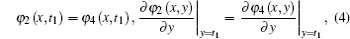
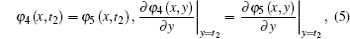
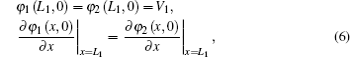
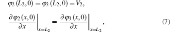
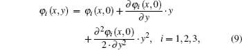
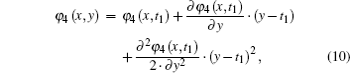
where K = ɛs/ɛox and ɛox is the dielectric constant for SiO2. Equation (2) is the vertical electric field at the semiconductor surface, which can be ignored. Equation (3) is the continuity of electric flux density across charge-free boundary. Equations (4)–(7) are the continuity equations of the potential and electric field along the boundaries of 2–4, 4–5, 1–2, and 2–3 regions, respectively. Equation (8) is the voltage condition applied to the device. The potential function can be Taylor expanded with respect to y coordinate up to the second-order terms as
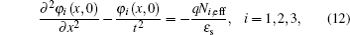
Substituting Eqs. (1)–(5) into Eqs. (9)–(11) leads to a general differential equation for the surface potential distribution function as
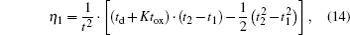
where N1,eff = N3,eff = Nnwell, and N2,eff = Nnwell − η1NPB + η2NT. The t, η1, and η2 denote the characteristic thickness value of drift region, the vertical doping factors of P-buried layer, and N-top layer, respectively, and are given as follows:
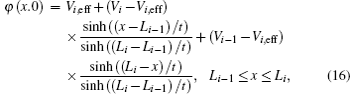
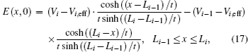
Solving Eq. (12) constrained by Eqs. (6)–(8) yields the distributions of surface potential and electric field as follows:
where i = 1, 2, 3 and Li − 1 ≤ x ≤ Li, Vi, eff = qNi, efft2/ɛs, V0 = 0, V3 = Vd, L0 = 0, L3 = Ld, and y = 0. The L1 and L2 are the positions of two boundaries between N-well and N-top layer. The V1 and V2 are the surface potentials of two boundaries between drift region and N-top layer and can be obtained from the condition (Eqs. (6) and (7)). It is worth nothing that the analytical expressions Eq. (16) and Eq. (17) are also applicable to other devices without being modified, such as single (NPB = 0, NT = 0), double (t1 = 0) and conventional triple RESURF (NT = 0) SOI LDMOS.
Solving the potential function partial respect to y and substituting it into Eqs. (1) and (2), the vertical electric field distributions can be described as
where
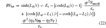
For the novel triple RESURF SOI LDMOS, the peak field at O2 in the N-top/N-well junction is larger than that at O3 in the N-well/N+ -drain junction because the P-buried layer is introduced and lengths of N-top layer and P-buried layer are close to the length of drift region. Therefore, there are two surface electric field peaks at O1 and O2. The lengths of P-buried layer and N-top layer are both almost equal to the length of drift region. So assuming L1 = 0 and L2 = Ld, the vertical breakdown can only occur at either O4 or O5. The electric field at O4 for the N-top/P-buried junction is larger than that at O2 due to the influence of vertical electric field at O4. Hence, the lateral breakdown voltage BVlat can be obtained from E(0,0) = Ec when the breakdown occurs at O1. The BVlat can be described as:
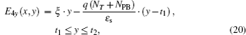
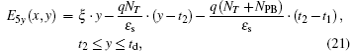
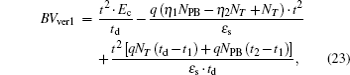
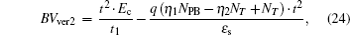
Besides, the vertical breakdown voltage BVver1 can be obtained from E2y(L1,t1) = Ec when the breakdown occurs at O4, and BVver2 can be obtained from E5y(L2,td) = Ec when the breakdown occurs at O5. The BVver1, BVver2, and BV are given as follows:
The analytical Qntop can be obtained when the N-well is fully depleted and the breakdown occurs at O4. The Qntop includes the charges of N-well and N-top layer. The vertical depletion extension d1 into the N-top layer can be given as follows:
The optimal Qntop for the N-top layer is expressed as
3. Results and discussion
In this paper, all the numerical results are obtained by 2D device simulator MEDICI and the analytical results are obtained by the analytical model. Figures 2(a) and 2(b) show the numerical and analytical profiles of surface potential and electric field for the novel and conventional triple RESURF SOI LDMOS, respectively. The novel and conventional triple RESURF SOI LDMOS obtain BV values of 450 V and 454 V, respectively. A fair accordance between the analytical and numerical profiles of surface potential and electric field may generally be found for the novel and conventional triple RESURF SOI LDMOS. For the novel triple RESURF SOI LDMOS, the heavily doped N-top layer results in a weak increase of the peak electric field in P-well/N-well junction. Because the P-buried layer is introduced and the lengths of N-top layer and P-buried layer are close to the length of drift region, the surface peak field at the N-top/N-well junction is larger than that at the N-well/N+ -drain junction. Figures 2(c) and 2(d) show the numerical and analytical profiles of surface potential and electric field for the single and double RESURF SOI LDMOS, respectively. The analytical expressions (16) and (17) can be simply used in single (NPB = 0, NT = 0) and double (t1 = 0) RESURF SOI LDMOS without being modified. The single and double RESURF SOI LDMOS obtain BV values of 445 V and 447 V, respectively. The analytical results of surface potential and electric field distributions for single and double RESURF SOI LDMOS show good agreement with the numerical simulation results.
Numerical and analytical profiles of surface potential and electric field of (a) novel triple RESURF SOI LDMOS, (b) conventional triple RESURF SOI LDMOS, (c) single RESURF SOI LDMOS, and (d) double RESURF SOI LDMOS in drift region.
Figure 3(a) shows the numerical results of BV, Ron,sp, and power figure of merit (FOM, defined as BV2/Ron,sp) versus Nnwell for the conventional triple RESURF SOI LDMOS with Ld = 35 μm, L1 = 2 μm, L2 = 31 μm, t1 = 1 μm, t2 = 2 μm, and td = 8 μm. The conventional triple RESURF SOI LDMOS has a correspondingly optimized NPB for any given Nnwell. Ron,sp decreases with the increase of Nnwell. With the increase of Nnwell from 3.2× 1015 cm−3 to 4.4× 1015 cm−3, BV is maintained at a similar value of above 450 V firstly. With the continuous increase of Nnwell from 4.4× 1015 cm−3 to 5.6× 1015 cm−3, BV decreases. With Nnwell = 4.4 × 1015 cm−3, the conventional triple RESURF SOI LDMOS obtains a BV of 454 V and a Ron,sp of 40 mΩ·cm2, yielding a highest FOM of 5.15 MW/cm2. Figure 3(b) shows the numerical results of BV and Ron,sp versus NT for the novel and conventional triple RESURF SOI LDMOS, and analytical maximum NT with Ld = 35 μm, L1 = 2 μm, L2 = 31 μm, t1 = 1 μm, t2 = 2 μm, td = 8 μm, and Nnwell = 4.4× 1015 cm−3. When NT = 0× 1016 cm−3, the device is a conventional triple RESURF SOI LDMOS which achieves a BV of 454 V and a Ron,sp of 40 mΩ·cm2. As NT increases, the N-top layer is formed. BV can maintain the same value, and Ron,sp decreases because an additional N-top layer introduces more majority carriers to significantly reduce Ron,sp, which alleviates the inherent tradeoff between Ron,sp and BV. Then, BV decreases when NT continues to increase. For any given NT, the device has a correspondingly optimized NPB when the drift region is fully depleted. When NT is 1.6 × 1016 cm−3, the novel triple RESURF SOI LDMOS can achieve a low Ron,sp of 31.3 mΩ·cm2 which is 22% lower than that of conventional triple RESURF SOI LDMOS at the same BV level. According to Eq. (27), with t1 = 1 μm, the analytical maximum NT is 1.56 × 1016 cm−3. When NT exceeds the value, BV decreases with the increase of NT.
(a) Numerical results of BV, Ron,sp, and FOM versus Nnwell for conventional triple RESURF SOI LDMOS, (b) numerical results of BV and Ron,sp versus NT for novel and conventional triple RESURF SOI LDMOS, and analytical maximum NT.
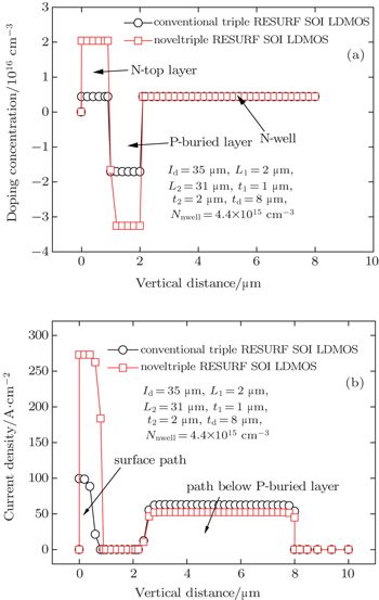
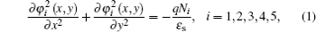
Figure 4(a) shows the numerical vertical doping profiles in the drift region for the novel and conventional triple RESURF SOI LDMOS with Ld = 35 μm, L1 = 2 μm, L2 = 31 μm, t1 = 1 μm, t2 = 2 μm, td = 8 μm, and Nnwell = 4.4× 1015 cm−3. With an extra N-top layer, the novel triple RESURF SOI LDMOS has more majority carriers at the surface of N-well than the conventional triple RESURF SOI LDMOS. Meanwhile, in order to keep charge balance for a high BV, the increased NPB is needed. The two structures have similar doping profiles of N-well below P-buried layer due to the same Nnwell. Figure 4(b) shows the corresponding current density distributions. Currents passing through the path below P-buried layer maintain for the two structures are approximately the same. However, current passing through the surface path of the novel triple RESURF SOI LDMOS is increased by near 175% in comparison with that of the conventional triple RESURF SOI LDMOS. Hence, the N-top layer provides a low on-resistance surface conduction path for the novel triple RESURF SOI LDMOS, contributing to a lower Ron,sp. Therefore, compared with the conventional triple RESURF SOI LDMOS, the novel triple RESURF SOI LDMOS with N-top layer can achieve a lower Ron,sp while maintaining a high BV.
Fig. 4. (a) Numerical vertical doping concentrations and (b) corresponding current density distributions in the drift region at x = 25 μm for the novel and conventional triple RESURF SOI LDMOS.
Figure 5 shows the numerical and analytical results of BV and numerical results of Ron,sp versus NPB at different values of NT for the novel triple RESURF SOI LDMOS when Ld = 35 μm, L1 = 2 μm, L2 = 31 μm, t1 = 1 μm, t2 = 2 μm, td = 8 μm, and Nnwell = 4.4 × 1015 cm−3. For the numerical results, with increase in NPB, BV has a maximum value when the N-well is fully depleted for any given NT. The Ron,sp is almost constant with the increase of NPB due to the nearly equivalent n-type impurity in the n-type drift region. As NT increases, Ron,sp is reduced for the same BV first. Then, BV decreases when NT continues to increase. The analytical BV values obtained from Eqs. (22)–(25), when the device is fully depleted, accord with the numerical results, showing the validity of the presented model.
Numerical and analytical results of BV and numerical results of Ron,sp versus NPB at different NT values for the novel triple RESURF SOI LDMOS.
Figure 6 shows the numerical results of BV versus Qntop at different values of t1 for the novel triple RESURF SOI LDMOS and the analytical maximum Qntop when Ld = 35 μm, L1 = 2 μm, L2 = 31 μm, td = 8 μm, and Nnwell = 4.4× 1015 cm−3. The thickness of P-buried layer in the simulations is 1 μm. With the increase of Qntop, the BV can be first maintained at a similar value and then decreases because of too high a dose of N-top layer. According to Eq. (27), the analytical maximum Qntop is ɛsEc/q. The analytical maximum Qntop is an upper theoretical bound for the dose of surface conduction path, which can guide the designer in achieving an optimal distribution of impurities in the drift region to optimize the tradeoff between the BV and Ron,sp. The critical electric field Ec is a weak function of the doping. With the decrease of t1, the concentration of the N-top layer will increase at the same Qntop, which causes the increase of Ec. So, the analytical maximum Qntop will increase with the decrease of t1. The analytical maximum Qntop values are obtained at different t1 values and are also shown in Fig. 6. With t1 = 1.0 μm, the analytical maximum Qntop is around 2.0 × 1012 cm−2. Hence, compared with the conventional triple RESURF SOI LDMOS, the novel triple RESURF SOI LDMOS can maintain a high BV and a lower Ron,sp with Qntop ≤ 2.0 × 1012 cm−2 at t1 = 1.0 μm.
Numerical results of BV versus Qntop at different t1 values for novel triple RESURF SOI LDMOS and the analytical maximum Qntop.
4. Conclusions
In this work, an analytical model for the surface potential and electric field distributions of the novel triple RESURF SOI LDMOS with N-top layer are presented. The corresponding analytical model for the surface potential and electric field distributions are also applicable to single, double and conventional triple RESURF SOI structures. Besides, the analytical BV and maximum Qntop are obtained. The analytical maximum Qntop is an upper theoretical bound which is useful to control the implantation doses and energy for the N-top layer. All the analytical results obtained from the given expressions can show fair agreement with the numerical results, indicating the validity of the presented model. Consequently, the proposed analytical model can be a good tool for the designer to optimize the novel triple RESURF SOI LDMOS with N-top layer. The novel triple RESURF SOI LDMOS can achieve a more optimized distribution of impurities in the drift region to further improve the tradeoff between BV and Ron,sp than the conventional triple RESURF SOI LDMOS.
Modeling of a triple reduced surface field silicon-on-insulator lateral double-diffused metal–oxide–semiconductor field-effect transistor with low on-state resistance
[Wang Yu-Ru1, Liu Yi-He1, Lin Zhao-Jiang1, Fang Dong1, Li Cheng-Zhou1, Qiao Ming1, 2, †, , Zhang Bo1]


 , Zhang Bo1]