School of Electronics and Information, Northwestern Polytechnical University, Xi’an 710072, China
† Corresponding author. E-mail: gfli@nwpu.edu.cn
Project supported by the National Natural Science Foundation of China (Grant No. 61504107) and the Fundamental Research Funds for the Central Universities, China (Grant Nos. 3102014JCQ01059 and 3102015ZY043).
1. IntroductionThe injection of spin-polarized electrons into semiconductor channels has attracted considerable interest recently.[1–3] To realize highly-efficient spin injection from a ferromagnetic electrode into a semiconductor channel, a highly-polarized spin injection source and a high-mobility semiconductor channel are required. The Heusler alloy Co2MnSi is a promising candidate as a spin injection source because of its theoretically predicted half-metallicity, that is, 100% spin polarization at the Fermi energy.[4] Indeed, Jourdan et al. have directly observed half-metallicity in the Heusler compound Co2MnSi in experiment.[5] Furthermore, germanium (Ge) is one of the promising semiconductor candidates because of its high bulk mobility for both electrons and holes. Thus, the combination of Co2MnSi and a Ge channel is expected to yield highly-efficient spin injection into Ge. However, in a ferromagnetic material (FM)/Ge junction, the acceptor- and donor-like interface states in the Ge can be easily occupied by carriers penetrating the material from the FM, which can lead to the accumulation of dipole moments at the interface.[6] Thus, the Fermi level can be pinned near the charge neutrality level (CNL).[6] As the CNL of Ge is close to the valence energy band, the Schottky barrier height (SBH) of the FM/Ge junction has a weak dependence on the metal work functions and the SBH of the FM/Ge junction is relatively large, resulting in a high resistance–area (RA) product. The realization of an FM/Ge junction with a low RA product is important for various Ge-based spintronic devices.
The previous reports have suggested that the insertion of a thin insulator between an FM and the Ge is a possible method for achieving Fermi-level depinning.[7–9] Here, depinning refers to the shift of the Fermi level relative to the original strong pinning position. However, the thin-insulator defects and amorphous state could lead to an inhomogeneous interfacial structure as well as variations in the bulk film quality and thickness, all of which introduce complications to the investigation of the origin of the Fermi-level pinning.
Graphene is a potential candidate for the insulator tunneling barrier for two primary reasons: (i) it provides a highly uniform, defect-free, and thermally stable thin layer (graphene has been shown to successfully prevent interdiffusion between a ferromagnetic material and a semiconductor annealed at high temperature);[10] and (ii) it exhibits poor conductivity perpendicular to the plane, although it is very conductive in-plane.[11] Cobas et al. have fabricated graphene-based magnetic tunnel junctions, in which the graphene functions as a tunnel barrier, thereby demonstrating clear magnetoresistance curves at room temperature.[12] Recently, van’t Erve et al. have reported that graphene can serve as a tunnel barrier for the spin injection from a NiFe thin film into a Si substrate using a three-terminal circuit geometry.[13] To date, however, very few studies have been published on the electrical properties of the Heusler alloy Co2MnSi/graphene/Ge heterostructure.
In the present study, we aim to investigate the effect of the graphene tunnel barrier in a Co2MnSi/graphene/Ge junction on the SBH. For this purpose, Co2MnSi thin films on Ge (001) substrates with graphene layers inserted are prepared using magnetron sputtering (for Co2MnSi thin films) and chemical vapor deposition (CVD, for graphene layers). The junctions are prepared using conventional photolithography and Ar milling, and the current versus voltage (I–V) characteristics of each junction are measured using a three-terminal circuit geometry. Subsequently, the thermionic emission model is used to quantitatively analyze the effect of the number of graphene layers on the SBH of the Co2MnSi/graphene/Ge heterostructure.
This paper is organized as follows. Section 2 describes the experimental methods; Section 3 presents our experimental results regarding the J–V characteristics of the Co2MnSi/graphene/Ge (001) heterostructures and an accompanying discussion; and Section 4 contains a summary of our results and conclusions.
2. Experimental methodThe layer structure examined in this study was comprised of (from the substrate side) graphene/Co2MnSi (20 nm)/Ru cap (5 nm) on a Ge (001) single-crystal substrate. The Ge substrate used here was an n-type as-doped substrate with 5 mΩ·cm resistivity. Following the removal of the native oxide using a diluted hydrofluoric acid solution, the substrate was cut into specimens with areas of 25 mm× 25 mm. The graphene was fabricated using CVD on a copper foil, and the resultant graphene/copper foil specimen was cut to sizes of 20 mm× 20 mm. The graphene surface was coated with photoresist to assist the subsequent wet-transfer process. The graphene/copper foil was immersed into ferric trichloride so that the copper was removed completely through etching, and the photoresist-coated graphene was then physically transferred onto the Ge (001) substrate. The sample was cleaned using a hydrofluoric acid solution, the photoresist was removed with acetone, and the resultant sample was finally washed using deionized water.
For samples requiring the transfer of two layers of graphene, once the first layer had been transferred, the photoresist was removed using acetone. Then the next graphene layer was transferred. Samples featuring single and double layers of graphene were examined in this study.
The prepared graphene/Ge (001) substrate was installed in a high-vacuum chamber with a base pressure of 5.0×10⁻⁴ Pa and a 20-nm-thick Co2MnSi thin film was then deposited via magnetron sputtering at room temperature (RT). The sample was subsequently annealed in-situ at a temperature Ta of 400 °C. After growth, junctions with sizes ranging from 30 μm× 30 μm to 150 μm× 150 μm were fabricated via conventional photolithography and Ar milling. The Cr/Au was deposited directly on the Ge for ohmic contact with a specimen size of 250 μm× 250 μm. The I–V characteristics of each junction were measured using a three-terminal circuit geometry.
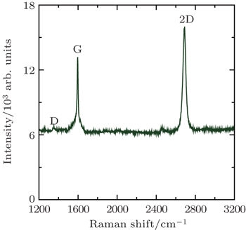
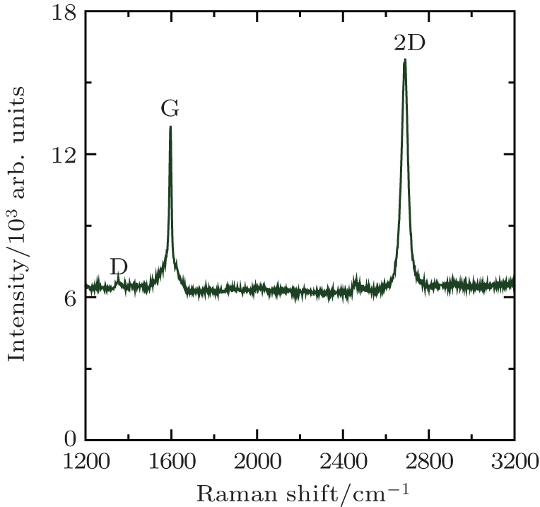
3. Results and discussionFigure 1 shows the Raman spectrum of a single graphene layer, which was fabricated on the Ge (001) substrate. The typical G and 2D peaks are observed at shifts of 1596 cm−1 and 2685 cm−1, respectively. The peak intensity ratio I2D/IG is approximately 1.62, and the relatively higher peak intensity ratio of the 2D peak compared with that of the G peak corresponds to the single-layer graphene profile. Furthermore, the full width at half maximum (FWHM) of the 2D peak is approximately 21 cm−1, which is very close to 25 cm−1 reported for perfect single-layer graphene. Although the D peak is observed at a shift of 1352 cm−1, which is related to a defect in the graphene layer, the peak intensity ratio ID/IG is approximately 0.06, which is appreciably small. This indicates that the prepared graphene is almost defect-free.[14]
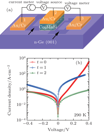
Figure 2(a) is a schematic diagram of a layer structure consisting of a Co2MnSi/graphene/Ge junction (labeled “2” in the figure and referred to as J2 hereafter), where the Cr/Au thin films were grown directly on the Ge substrate for ohmic contact with junctions 1 and 3. The I–V characteristics of J2 were measured using the three-terminal circuit geometry. A bias voltage V was applied between terminals 1 and 2, a current meter was used to measure the current across J2, and the V across J2 was obtained through measurement of the V between terminals 2 and 3. For a negative (positive) bias, the Co2MnSi/graphene/Ge junction was reverse (forward) biased.
Figure 2(b) shows the typical J–V characteristics of the Co2MnSi/graphene/Ge (001) heterostructures with different numbers of graphene layers at RT. Following the insertion of a single graphene layer (t = 1), the reverse-biased current increases in comparison to the Co2MnSi/Ge Schottky diode (t = 0), indicating that the Fermi level is depinned. However, when two graphene layers are used (t = 2), the reverse- and forward-biased currents decrease. Most importantly, the J–V characteristics are near symmetric with respect to the bias polarity, and the transport mechanism changes from rectifying (for Co2MnSi grown directly on the Ge (001) substrate) to symmetric tunneling following the insertion of two graphene layers. Moreover, the RA products of the contacts at a reversed bias of –0.20 V are 0.78 Ω·cm2, 0.19 Ω·cm2, and 1.2 Ω·cm2 for t = 0, 1, and 2, respectively.
For a quantitative analysis of the effect of the graphene layer insertion on the SBH of the Co2MnSi/graphene/Ge junction, the thermionic emission model is adopted.[15] This model is expressed as
where
A* is the Richardson constant,
T is the temperature,
q is the electron charge,
k is the Boltzmann constant,
ϕb is the effective SBH,
n is an ideality factor, and
V is the applied bias voltage.
For V ≫ kT/q, 1 −exp(–qV/kT) ≈ 1 (kT/q = 18 eV–26 mV for T ranging from 210 K to 300 K). Thus, equation (1) can be expressed as

For a plot of ln(
J/
T2) versus 1/
T, also called the Richardson plot, a linear line is found with a slope of
a = −(
q/
k)(
ϕb −
V/
n). In this study, a set of
a values were obtained for different
V. Then, plotting
a as a function of
V, a linear curve with slope –(
q/
k)(1/
n) was obtained along with a
y-axis intercept of
ϕb.
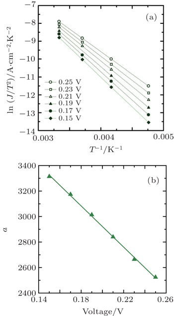
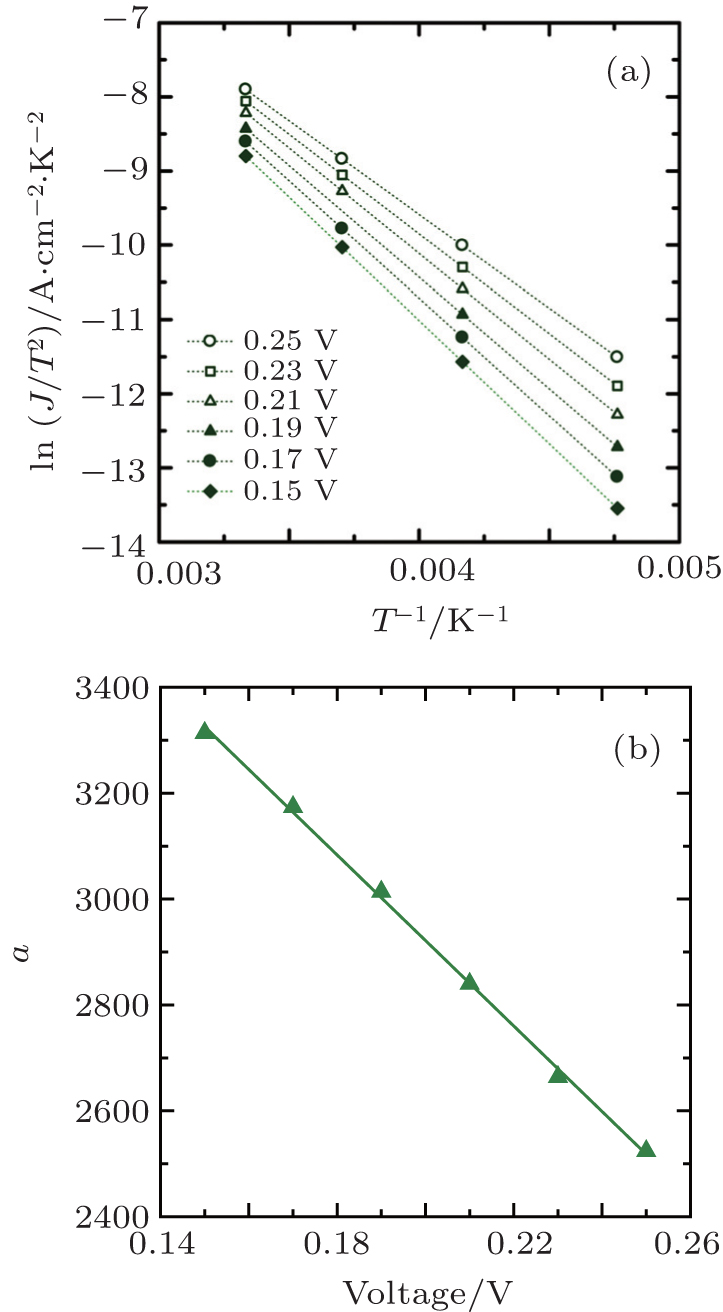
Figure 3(a) shows the Richardson plots of the Co2MnSi/single-graphene (t = 1)/Ge (001) junction for V = 0.15 V–0.25 V. The a is extracted from the linear fitting of each plot and then plotted as a function of V in Fig. 3(b). From the linear fitting of the latter plot, n and ϕb are found to be 1.45 and 0.39 eV, respectively. Note that lnA* is not considered in the calculation of the SBH for the Co2MnSi/graphene/Ge (001) junction; this is because the additional contribution from the tunneling probability through the graphene could be viewed as a modification of the conventional A*.[16]
The SBH and n values of the Co2MnSi/graphene/Ge (001) junctions with different numbers of graphene layers are extracted and listed in Table 1. For the Co2MnSi grown directly on the Ge (001) substrate, n is slightly larger than expected at 1.0. This may be due to the high doping concentration of the n-Ge substrate. The n increases with increasing t, which is consistent with a change in the dominant transport mechanism from thermionic emission (n ≈ 1) to an additional tunneling process (n > 1).[16] Moreover, the SBH exhibits a negative dependence on t, which is consistent with the metal-induced gap states (MIGS) model.[17,18] Very little interface modulation of the Schottky junction behavior was observed for the Co2MnSi/single graphene/Ge junction.
Table 1.
Table 1.
 Table 1. The Schottky barrier height and ideality factor (n) of Co2MnSi/graphene/Ge (001) junctions with different graphene tunnel barrier thicknesses. .
| The number of single-layer graphene |
Schottky barrier height/eV |
Ideality factor n |
| 0 |
0.61 |
1.12 |
| 1 |
0.39 |
1.45 |
| 2 |
0.34 |
2.41 |
| Table 1. The Schottky barrier height and ideality factor (n) of Co2MnSi/graphene/Ge (001) junctions with different graphene tunnel barrier thicknesses. . |
It is well known that MIGS are formed by tailing of the wave function into the semiconductor band-gap. Therefore, it is very likely that tailing suppression due to the presence of the ultrathin graphene layer caused the change in the SBH. However, when two layers of graphene were inserted between Co2MnSi and the Ge channel, the tunneling dominated the transport mechanism. Thus, this result provides an evidence that the MIGS are the most plausible mechanism for the strong Fermi-level pinning at the Co2MnSi/Ge interface. As the graphene-layer thickness increases, the SBHs decrease significantly and the I–V characteristics become almost symmetric with respect to the bias polarity for the Co2MnSi/double-graphene (t = 2)/Ge junction, which is promising as regard to the realization of spin injection and detection from highly spin-polarized Co2MnSi thin films to Ge channels featuring high electron and hole mobility.
4. ConclusionThe effect of the inserted graphene layer on the Schottky barrier height of a Co2MnSi/graphene/Ge junction was investigated with one or two graphene layers. It was found that the Fermi level was depinned and the SBH was significantly decreased (from 0.61 eV to 0.34 eV) following the insertion of a graphene layer. Furthermore, the measured SBH depended on the number of graphene layers, which is consistent with the metal-induced gap states model. Our results demonstrate that graphene insertion can be useful for the realization of spin injection and detection from highly spin-polarized Co2MnSi thin films to Ge channels featuring high electron and hole mobility.


 , Hu Jing, Lv Hui, Cui Zhijun, Hou Xiaowei, Liu Shibin, Du Yongqian]