Du Liang-Liang, Li Quan, Li Shao-Xian, Hu Fang-Rong, Xiong Xian-Ming, Li Yan-Feng, Zhang Wen-Tao, Han Jia-Guang. Polarization-independent terahertz wave modulator based on graphene-silicon hybrid structure. Chinese Physics B, 2016, 25(2): 027301
Permissions
Polarization-independent terahertz wave modulator based on graphene-silicon hybrid structure
Du Liang-Liang1, 2, Li Quan2, Li Shao-Xian2, Hu Fang-Rong1, Xiong Xian-Ming1, Li Yan-Feng1, Zhang Wen-Tao1, †, , Han Jia-Guang2, ‡,
College of Electrical Engineering and Automation, Guilin University of Electronic Technology, Guilin 541000, China
Center for Terahertz Wave, Key Laboratory of Opto-electronic Information Technology, Ministry of Education, College of Precision Instrument and Optoelectronics Engineering, Tianjin University, Tianjin 300072, China
Project supported by the National Natural Science Foundation of China (Grant No. 61565004), the Natural Science Foundation of Guangxi Zhuang Autonomous Region, China (Grant Nos. 2013GXNSFDA019002 and 2014GXNSFGA118003), the Guangxi Scientific Research and Technology Development Program, China (Grant No. 1598017-1), the Guilin Scientific Research and Technology Development Program, China (Grant Nos. 20140127-1 and 20150133-3), and the Special Funds for Distinguished Experts of Guangxi Zhuang Autonomous Region, China.
Abstract
Abstract
In this study, we propose and demonstrate a broadband polarization-independent terahertz modulator based on graphene/silicon hybrid structure through a combination of continuous wave optical illumination and electrical gating. Under a pump power of 400 mW and the voltages ranging from –1.8 V to 1.4 V, modulation depths in a range of –23%–62% are achieved in a frequency range from 0.25 THz to 0.65 THz. The modulator is also found to have a transition from unidirectional modulation to bidirectional modulation with the increase of pump power. Combining the Raman spectra and Schottky current–voltage characteristics of the device, it is found that the large amplitude modulation is ascribed to the electric-field controlled carrier concentration in silicon with assistance of the graphene electrode and Schottky junction.
Terahertz waves, whose frequencies lie between the microwave and optical range, inherit features from both photonics and electronics. The vibration and rotation levels of many polar molecules fall within the terahertz band and therefore terahertz waves can be used for substance detection. Owing to the low photon energy, terahertz waves are non-ionizing and safe. Compared with the modern wireless communication band, terahertz communication has a high rate, allowing greater capacity wireless transmission of information in real time. It is because of these outstanding physical properties that the terahertz waves have found many important applications in the biomedical field, wireless communication, radar imaging, etc.[1–4] Those applications in turn call for the urgent development of various terahertz functional devices, such as modulators. Modulators are well established and considered as standard devices in the optical realm, but in the terahertz frequency regime, there is an increasing demand for high-efficient, fast and versatile active modulators. The modulator enables information to be encoded on terahertz waves, thus providing potential applications in imaging, telecommunication, and beam shaping. Graphene, an ideal two-dimensional (2D) material with unique band structure and electron transport properties, shows excellent electrical and optical properties and good compatibility.[5] In the terahertz range, the intraband transitions are the dominant cause of terahertz response of graphene, which makes the graphene widely used in the active terahertz modulators. Compared with other modulation strategies, such as the temperature control of VO2,[6] the optical control of silicon,[7] and the electrical control of GaAs,[8] the graphene shows high flexibility, easy integration, fast response, and other outstanding features. Ju et al. studied the tunable plasmon excitations and light-plasmon coupling at terahertz frequencies in graphene micro-ribbon arrays, where over 13% of the absorption modulation depth was experimentally demonstrated at the plasmon resonance at room temperature.[9] Ren et al. exploited the tunability of the Fermi surface of the graphene on a 300-nm-thick SiO2 layer on the silicon substrate (5 Ω·cm∼10 Ω·cm) and realized terahertz modulation, and observed the charge neutral point (CNP).[10] Sensale-Rodriguez et al. realized a terahertz transmittance modulation depth of 15% and reflectance modulation depth of 64% by the electrical control of the conductivity of single-layer graphene with the same pattern but different doping concentration.[11,12] The monolayer graphene on a layer of hexagonal metallic meta-atoms embedded between the extraordinary optical transmission electrodes[13] can modulate the amplitude of the transmitted terahertz wave up to 47% at the resonance frequency.[14,15] Gao et al. reported a ∼50% amplitude modulation of terahertz waves with gated single-layer graphene by use of extraordinary transmission through metallic ring apertures placed right above the graphene layer.[16] Mao et al. presented a broadband terahertz wave modulator with improved modulation depth by cautiously selecting the gate dielectric materials in a large-area graphene-based field-effect transistor, which achieved a modulation depth of 22% in a frequency range from 0.4 THz to 1.5 THz.[17] Among these previous studies, although the interaction between the light and the graphene can be significantly enhanced by using the resonant metamaterial structure, such a modulator is still limited by its operation bandwidth and is polarization-sensitive. Additionally, the fabrication of multilayer structure is complicated and costly, and the high voltage is mostly required.
On the basis of the high conductivity and low insertion loss of the graphene, here we present an optically pumped and voltage-controllable terahertz modulator. With the increase of the pump power of the 445-nm continuous wave (CW) laser, the modulation depth increases and a transition from unidirectional modulation to bidirectional modulation is observed. When the photoexcitation power is 400 mW, this modulator exhibits maximum transmission modulation depths in a range of –23%–62% at frequencies ranging from 0.25 THz to 0.65 THz and small bias voltages ranging from –1.8 V to 1.4 V.
2. Experiment
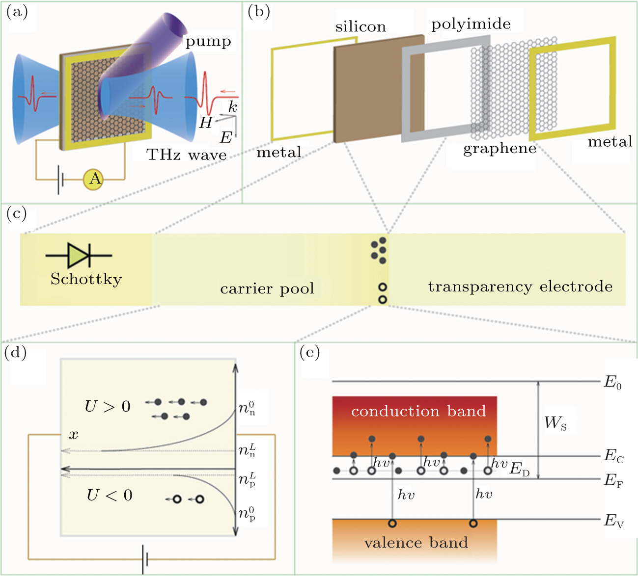
The measurement schematic and detailed structure of the terahertz modulator are shown in Figs. 1(a) and 1(b). The fabrication process is briefly described as follows. A 5-μm-thick ring-shaped polyimide (PI) electric insulation layer was spin-coated on the 500-μm-thick n-type silicon substrate. Then monolayer graphene grown by chemical vapor deposition[18] was transferred from the copper foil onto the PI/Si substrate by using standard wet transfer techniques.[19] The graphene completely covered the PI square ring layer. Using physical vapor deposition, two 200-nm-thick aluminum square rings were then carefully made on both sides of the graphene–silicon hybrid structure as two electrodes to apply a bias voltage to the modulator. Under different pump powers of a 445-nm CW laser and different bias voltages, the transmitted and reflected terahertz spectra of the device were measured by using the fiber-based terahertz system (T-Ray 5000 by Advanced Photonix, Inc.). This terahertz system can be easily operated in reflection measurement mode with using its collinear adapter. The pump light was incident at a 45° angle and covered the terahertz spot. To obtain the voltage–current characteristic, the electric current through the sample was recorded by a multimeter during the measurements.
Fig. 1. (a) Measurement schematic diagram, (b) detailed structure, and (c) equivalent model of the proposed structure; (d) distribution of carrier concentration in silicon under DC bias voltage; (e) electron transition under photoexcitation.
Raman spectra of the monolayer graphene of the modulator under different optical pump powers and bias voltages were acquired by a Renishaw inVia Raman spectrometer. The Raman excitation light was 514 nm and the excitation power was about several milliwatts. A 50× object lens was used and the integration time of the Raman spectra measurement was 300 s for a spectral range of 1000 cm−1∼3000 cm−1.
3. Results and discussion
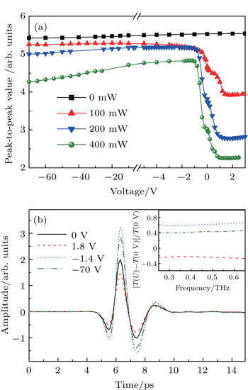
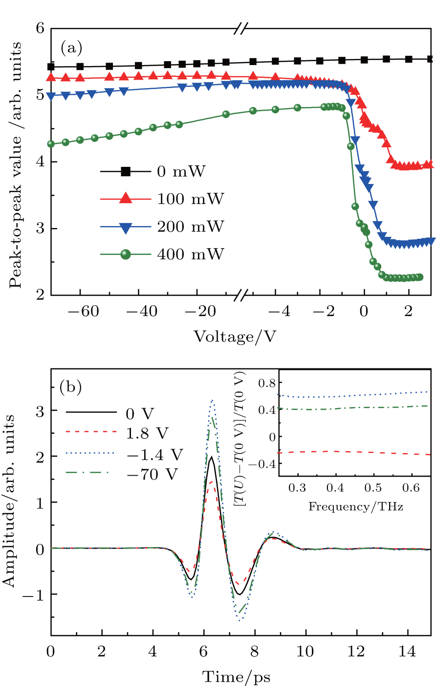
The proposed structure could be actively controlled by the optical power of the pump light and the bias voltage. Figure 2(a) shows the peak-to-peak values of the transmitted terahertz time-domain signals each as a function of bias voltage under different laser photoexcitation powers (0, 100, 200, and 400 mW). In the absence of laser pumping, the terahertz transmission changes slightly with the bias voltage varying from –70 V to 3 V. When the modulator is illuminated by 445-nm laser, a fast decrease of the peak-to-peak value is observed from –1 V to 1 V and then it reaches a saturated value when the voltage is above 1 V as shown in Fig. 2(a). With the further increase of the illuminating power, a modulation is observed by applying the negative bias voltage (see the curves for 200 mW and 400 mW in Fig. 2(a)).
Fig. 2. (a) Peak-to-peak values of terahertz time-domain signals transmitted through the sample controlled by the bias under different photoexcitation powers; (b) transmitted terahertz time-domain signals at various gate bias voltages under a photoexcitation power of 400 mW. Inset shows corresponding modulation depths with taking the amplitude transmission at 0 V (T(0 V)) as a reference.
Figure 2(b) shows the transmitted terahertz time-domain signals of the sample at –70, –1.4, 0, and 1.8 V bias voltages under an excitation power of 400 mW. The chosen structure reaches the CNP at –1.4 V, where the photoinduced holes compensate for the electrons in n-type silicon, and the terahertz transmission arrived at its maximum. The modulation depth is defined as |(T(U) – T(0 V))/T(0 V)|, where T(U) is the terahertz amplitude transmission at a bias voltage U. The modulation depth in a frequency range of 0.25 THz–0.65 THz is shown in the inset of Fig. 2(b). The modulation depth exhibits flat and broadband characteristics. Modulation depths of –23%∼62% in the –1.4 V∼1.8 V voltage range are achieved. A larger modulation depth can be expected if the photo-generated carrier concentration can be increased.
An equivalent model of the terahertz modulator is proposed as shown in Fig. 1(c). The modulator consists of a terahertz wave transparent electrode (graphene), a carrier pool (n-type silicon), and a Schottky junction formed by the ring-shaped metal electrode on the back side of the n-type silicon. As shown in Fig. 1(e), electrons at a donor level and in a valence band of the silicon will be excited into the conduction band when the silicon is illuminated by 445-nm CW laser (the band gap of silicon is 1.2 eV and is smaller than the exciting photon energy of 2.78 eV). Photoelectric effect cannot happen because the exciting photon energy is smaller than the work function of silicon (Ws > 4.05 eV). Depending on the direction of the bias voltage, the photo-induced holes and hot electrons can diffuse to the silicon or graphene. The carrier concentration in silicon can be tuned so that the silicon acts as a carrier pool. Owing to the high electrical conductivity of graphene and the improved conductivity of the optically excited silicon layer, we speculate that it is difficult for net charges to be accumulated at the graphene/silicon interface. Thus a strong local electric field cannot be formed and the graphene Fermi level will not be tuned either.[20,21] The Raman experimental results verify our speculation. Because the Fermi level of the graphene cannot be tuned, the graphene will not modulate the terahertz wave under such a situation. Instead, the low terahertz insertion loss of graphene makes it a good terahertz transparent electrode.[11] The PI layer between silicon and graphene prevents photoexcitation carriers from transmitting directly from the silicon surface to the metal ring, and thus avoiding the bypass carrier loss and improving the depth of modulation. The square metal ring on the back side of the silicon surface and the n-type silicon form a Schottky junction.
Figure 3 shows the Raman spectra of the proposed monolayer-graphene sample and the double-layer-graphene sample under photoexcitation of 100 mW and zero bias. The inset in Fig. 3(a) shows the spectra of the 2D peak at different bias voltages (–60 ∼ 5 V) with a 445-nm light excitation of 100 mW. A small shift of the frequency less than 2 cm−1 of the 2D peak is observed. We also fabricate another similar sample except that the monolayer graphene was replaced by double layer graphene. However, the frequency shift phenomenon of the 2D peak disappears for the sample of double-layer graphene as shown in the inset of Fig. 3(b). The different Raman responses between the monolayer and double graphene may be ascribed to the difference between their conductivities. The higher conductivity of double graphene makes the charges more efficiently transport to the metal ring and the accumulated charges at the double graphene/silicon interface can be neglected. As a result, the Fermi level is kept unmoved. On the other hand, because of the lower conductivity of monolayer graphene, a small number of charges may accumulate at the monolayer graphene/silicon interface and the induced weak local electric field thus gives rise to a small disturbance of the graphene Fermi level, which results in a small frequency shift of the 2D peak.[22,23] However, the disturbance in the Fermi level of the monolayer graphene cannot lead to a significant modulation of the terahertz wave.
Fig. 3. Raman spectra of (a) the proposed monolayer-graphene sample and (b) the double-layer-graphene sample under photoexcitation of 100 mW and zero bias. Insets show Raman shifts of the 2D peak under photoexcitation of 100 mW but different bias voltages (–60 V–5 V).
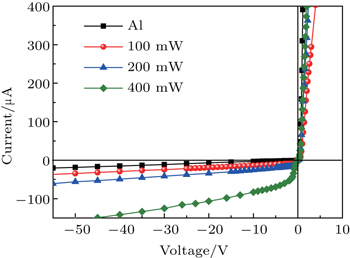
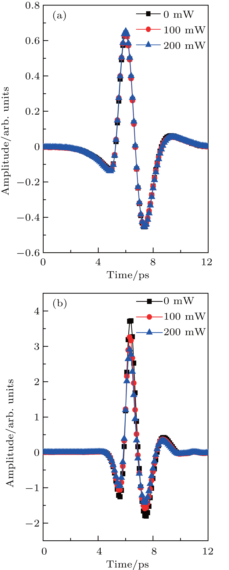
Figure 4(a) shows the terahertz reflection signals at different pump powers. The reflection change Δr is almost zero, which indicates that the transmission change Δt induced by the graphene could be neglected.[24,25] Figure 4(b) shows an obvious decrease of the transmitted signals with the increase of the pump power. This modulation is induced by increasing the carrier concentration in silicon when illuminated by 445-nm laser. Figure 5 shows the voltage-current characteristics of the modulator under different optical excitation powers. For comparison, a similar structure, in which the graphene on the modulator is replaced by a 200-nm-thick aluminum film, is measured. The aluminum sample exhibits the best current–voltage characteristic of a diode as shown by the curve with square markers. The direction of the bias voltage and the current–voltage curves indicate that the Schottky junction of either the graphene sample or the aluminum sample is formed between the silicon and the back metal ring electrode. With the increase of the pump power, the carrier concentration of the silicon increases and the Ohmic contact resistance decreases, resulting in the improved forward conduction and deteriorated reverse-blocking ability as shown in Fig. 5. The increasing reverse leakage current makes possible the modulation of the terahertz wave by a negative bias voltage.
Fig. 4. (a) Reflected and (b) transmitted terahertz time-domain signals from the proposed structure under different photoexcitation powers (0, 100, 200 mW) with zero bias.
Fig. 5. Voltage–current characteristic curves of the metallic sample (monolayer graphene is replaced by a 200-nm thick aluminum film) without optical pump are compared with those of the proposed sample under photoexcitation powers of 100, 200, and 400 mW.
The low-doped n-type silicon in the experiments is a non-degenerate semiconductor and the carrier distribution approximately obeys the Boltzmann law. The carrier diffusion coefficient in silicon can be described by Einstein’s relation as D = (kT/q)μ, where k is the Boltzmann constant, T is the temperature, q is the elementary charge, and μ is the carrier mobility. Owing to the carrier recombination during their diffusion, the concentration of the nonequilibrium carriers of the excited silicon decreases from the surface to the internal (Fig. 1(d)). According to the continuity equation, we can obtain the electron (hole) concentration at a distance x inside the silicon from the optical excitation surface as
The conductivity of the silicon can be further expressed as
Here τ is the non-equilibrium carrier lifetime and L is the thickness of the silicon. and n̄ are the concentrations of carriers (electrons and holes) at the front, at the rear surfaces of silicon, and the average carrier concentration, respectively. U and Us are the applied bias voltage and voltage drop across the Schottky junction, respectively.
When the Schottky junction is forward-biased, the voltage drop Us is very small, so the applied bias voltage mainly acts on the silicon substrate. The electric field inside the silicon rises rapidly with increasing voltage. The photoinduced holes transmit to the electrode directly while the electrons diffused into the silicon assisted by the electric field. The electric field enhances the electron diffusion, and the electron concentration n(x) is increased. Therefore the substrate carrier concentration n̄ increases rapidly and causes a rapid attenuation of the terahertz transmission, corresponding to the modulation in a voltage range of 0 V–1 V shown in Fig. 2(a). Owing to the limited carrier generation rate and the limited concentration of the photo-generated carriers, the average carrier concentration will reach a saturation state. So the transmittance of terahertz waves would eventually be stabilized, corresponding to the performance at the bias voltage above 1 V shown in Fig. 2(a).
When the Schottky junction is reverse-biased, holes would diffuse into the silicon and recombine with electrons, causing the carrier concentration to decrease. The terahertz transmission increases and reaches a maximum at CNP. When the voltage continuously increases in the negative direction, the number of diffusing holes in silicon begins to increase and the conductivity of silicon begins to increase. More photoinduced carriers are generated under a higher optical pump power, and a larger increase of the conductivity of silicon will occur at the same voltage. Thus the transmitted terahertz signal decreases faster at a higher optical pump power. Compared with the strong modulation in a voltage range from –1 V to 1 V, the slight modulation by the voltage below CNP shown in Fig. 2(a) can be explained by the slower increase of the electric field in silicon because the applied bias voltage mainly drops in the Schottky junction. A larger modulation slope under a higher optical pump power is observed.
4. Conclusions
In this paper, a broadband and polarization-independent terahertz amplitude modulator based on monolayer graphene on silicon in combination with a Schottky junction is presented. The Schottky junction is used to control the electric field in silicon. By dynamically adjusting the diffusion of the photoinduced carriers in graphene and silicon and thus controlling the carrier concentration in silicon, the modulator shows a significant terahertz amplitude modulation. Under 100-mW photoexcitation of 455-nm CW laser, the modulator operates in the unidirectional modulation mode. Under 400-mW photoexcitation, the modulator exhibits voltage-controlled bidirectional modulation and reaches maximum transmission modulation depths of –23%–62% in the 0.25 THz–0.65 THz range. The modulation depth becomes larger with the increasing of pump power. The modulator can be incorporated into metamaterials to further improve the modulation depth and modulation rate. The proposed design with detailed analysis of carrier concentration in the graphene/semiconductor hybrid structure is great helpful for realizing new efficient active terahertz modulators.


 , Han Jia-Guang2, ‡,