Yang Jing, Zhao De-Gang, Jiang De-Sheng, Chen Ping, Liu Zong-Shun, Zhu Jian-Jun, Le Ling-Cong, Li Xiao-Jing, He Xiao-Guang, Zhang Li-Qun, Yang Hui. Different variation behaviors of resistivity for high-temperature-grown and low-temperature-grown p-GaN films. Chinese Physics B, 2016, 25(2): 027102
Permissions
Different variation behaviors of resistivity for high-temperature-grown and low-temperature-grown p-GaN films
Yang Jing1, Zhao De-Gang1, †, , Jiang De-Sheng1, Chen Ping1, Liu Zong-Shun1, Zhu Jian-Jun1, Le Ling-Cong1, Li Xiao-Jing1, He Xiao-Guang1, Zhang Li-Qun2, Yang Hui1, 2
State Key Laboratory on Integrated Optoelectronics, Institute of Semiconductors, Chinese Academy of Sciences, Beijing 100083, China
Suzhou Institute of Nano-tech and Nano-bionics, Chinese Academy of Sciences, Suzhou 215123, China
Project supported by the National Natural Science Foundation of China (Grant Nos. 61474110, 61377020, 61376089, 61223005, and 61176126), the National Natural Science Fund for Distinguished Young Scholars, China (Grant No. 60925017), the One Hundred Person Project of the Chinese Academy of Sciences, and the Basic Research Project of Jiangsu Province, China (Grant No. BK20130362).
Abstract
Abstract
Two series of p-GaN films grown at different temperatures are obtained by metal organic chemical vapor deposition (MOCVD). And the different variation behaviors of resistivity with growth condition for high- temperature(HT)-grown and low-temperature(LT)-grown p-GaN films are investigated. It is found that the resistivity of HT-grown p-GaN film is nearly unchanged when the NH3 flow rate or reactor pressure increases. However, it decreases largely for LT-grown p-GaN film. These different variations may be attributed to the fact that carbon impurities are easy to incorporate into p-GaN film when the growth temperature is low. It results in a relatively high carbon concentration in LT-grown p-GaN film compared with HT-grown one. Therefore, carbon concentration is more sensitive to the growth condition in these samples, ultimately, leading to the different variation behaviors of resistivity for HT- and LT-grown ones.
Gallium nitride (GaN) based materials and their MOCVD growth technology have attracted a great attention due to their successful applications in light emitting devices.[1–3] In the development of these lighting devices, the fabrication of high quality p-type GaN is a key requirement.[4,5] However, the low hole concentration and high resistivity of p-type GaN have become one bottleneck to limit the performance of light emitting device due to the high activation energy of Mg acceptors and the compensation effects in Mg-doped GaN.[6] In recent years, with the development of long wavelength light emitting devices, such as green light emitting diode (LED) and laser diode (LD), the p-type GaN layer should be grown at low temperature (< 1000 °C) to protect the segregation and structural degradation of high indium content InGaN/GaN multi-quantum well (MQW) layers from being segregated and degraded, which further increases the difficulty in growing high-quality p-GaN layers because the low-temperature (LT)-grown p-type GaN film often shows a higher resistivity than expected. Several reports[7–10] demonstrated the effects of growth conditions, such as Mg source flow rate, V/III ratio, and pressure, on electrical properties of high-temperature(HT)-grown p-GaN films. However, the researches of LT-grown p-GaN films are rare. In this paper, two series of Mg-doped GaN films are grown in a MOCVD system at different growth temperatures, and the variations of resistivity with growth parameters, i.e., NH3 flow rate and reactor pressure are investigated for HT- and LT-grown p-GaN layers, respectively. Finally, the reasons for the different variation behaviors of resistivity between HT and LT grown ones are analyzed in detail.
2. Experiment
Ten Mg-doped GaN films (∼1-μm thick) were grown on the unintentionally doped GaN layer in a vertical MOCVD system with using trimethylgallium (TMGa), ammonia (NH3) and bis- (cyclopentadienyl-) magnesium (Cp2Mg) as the metal organic precursors for Ga, N, and Mg, respectively. These samples were divided into two series according to their growth temperatures: 950 °C for LT-grown p-GaN films (denoted as L1–L5) and 1050 °C for HT-grown p-GaN films (marked as H1–H5). The Mg doping concentration was mainly adjusted by Cp2Mg flow rate and a constant Mg concentration of 1 × 1019 cm−3 was doped in both LT and HT GaN films. The other growth parameters of these samples were listed in Table 1. The post thermal annealing was carried out in a nitrogen environment at a temperature of 800 °C for 20 min to de-passivate the Mg–H complexes. The Mg, C, O concentrations of the GaN films were checked by secondary ion mass spectroscopy (SIMS) measurements the resistivity and surface morphology are measured by using a room temperature Hall system and atomic force microscope (AFM), respectively.
Values of growth temperature (GT), growth pressure (GP), growth rate (GR), NH3, TMGa flow rate, and resistivity for Mg-doped GaN films H1∼H5, L1∼L5. The unit 1 Torr = 1.33322 × 10² Pa.
Sample
GT/°C
GP/Torr
NH3/sccm
TMGa/sccm
GR/(μm/h)
Resistivity/Ω·cm
Series I
H1
1050
100
3000
36
1.6
1.3
H2
1050
100
5000
36
1.65
1.38
H3
1050
100
7000
36
1.6
1.91
H4
1050
100
1500
36
1.6
1.37
H5
1050
200
3000
36
1.0
1.22
Series II
L1
950
100
3000
18
1.46
1650
L2
950
100
3000
12
0.8
528
L3
950
100
6000
12
0.8
1.5
L4
950
100
8000
12
0.8
10.9
L5
950
200
3000
12
0.8
3
3. Results and discussion
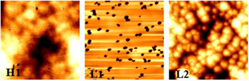
Two series of Mg-doped GaN films with different growth temperatures are grown. Their growth conditions (growth temperature (GT), growth pressure (GP), growth rate (GR), NH3, TMGa flow rate), and resistivity are listed in Table 1. It can be seen that in order to grow LT p-GaN layers with the same growth rate as HT ones, the TMGa flow rate must be reduced. This may be due to the weak pre-reaction between TMGa and NH3 at low temperature. The surface morphologies of all p-GaN layers are measured and some of them (H1, L1, and L2) are shown in Fig. 1.
Fig. 1. Surface morphologies of samples H1, L1, and L2 measured by AFM.
It is interesting to note that the surface morphologies of samples H1 and L1 are very different even though the growth rates of these two samples are nearly the same. For sample L1, many holes are observed on its surface, and therefore the surface root mean square (RMS) roughness of L1 is much larger than that of H1. It indicates that low growth temperature is a detrimental condition for forming good surface of Mg-doped GaN films due to the low atom mobility at low temperature. In order to obtain the LT-grown p-GaN layer with a good surface, the growth rate is further reduced (samples L2 and L3) from 1.46 μm/h to 0.8 μm/h. It is found that the surface root-mean-square (RMS) roughness decreases from 5.68 nm for sample L1 to 1.29 nm for sample L2, a value close to 1.25 nm of H1. Therefore, a relatively low TMGa flow rate is necessary for growing LT-grown p-GaN films. However, the resistivity of LT-grown p-GaN is still much larger than that of H1, implying that the characteristics of HT- and LT-grown p-GaN films may be different. In order to obtain the low resistivity LT-grown p-GaN film, next, the variation behaviors of LT- and HT- grown p-GaN with growth condition are investigated in detail.
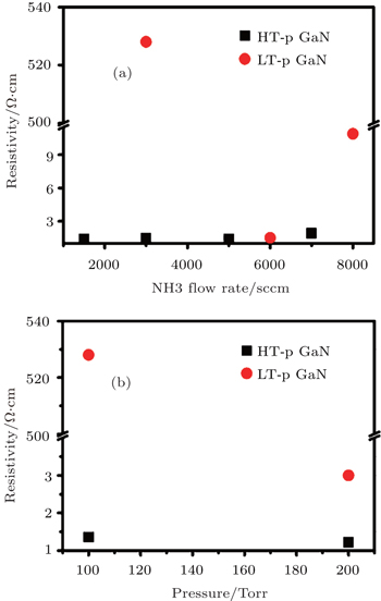
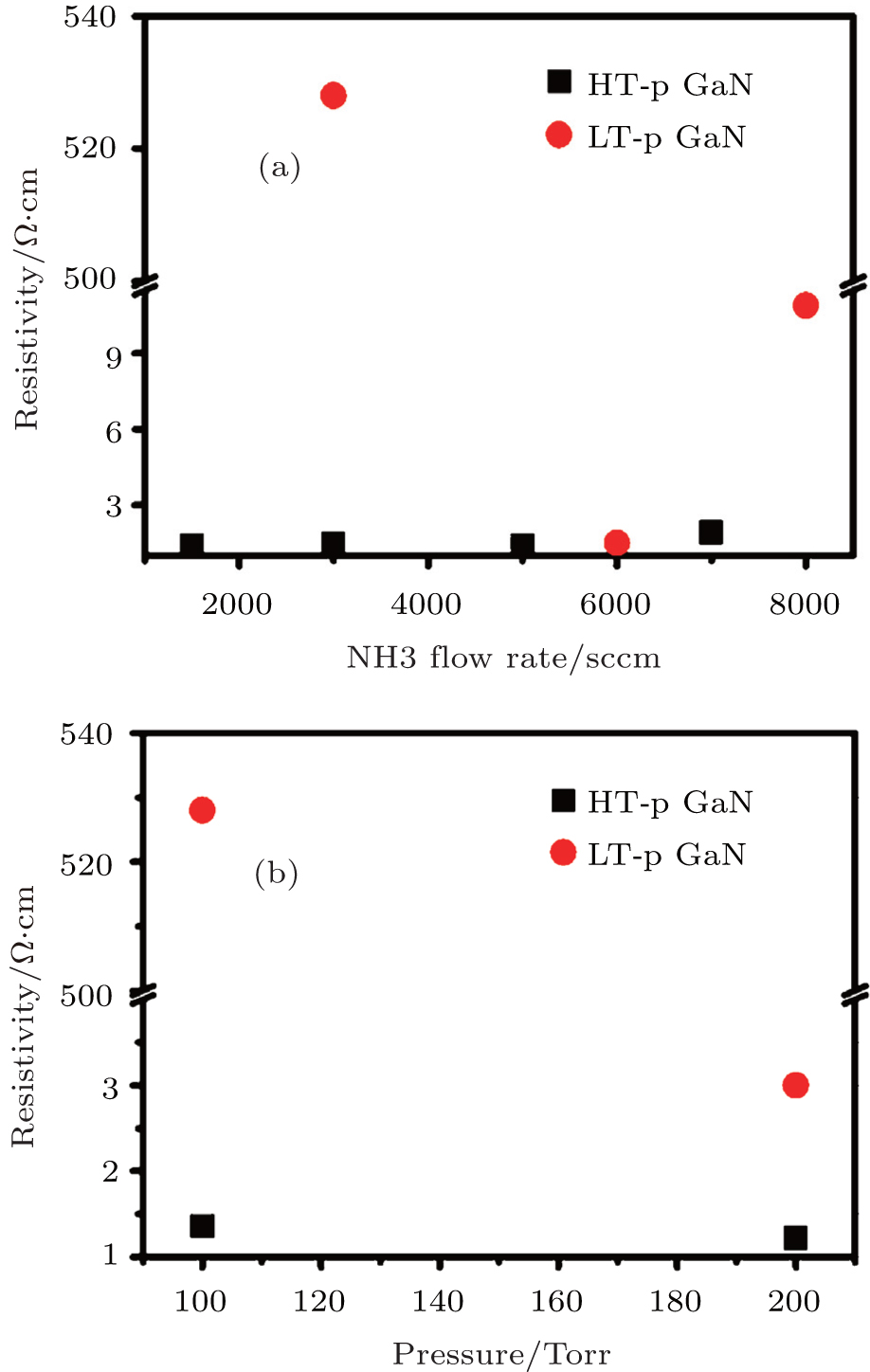
The resistivity of all p-GaN films are measured by room temperature (RT) Hall system and the dependences of resistivity on NH3 flow rate and reactor pressure are shown in Fig. 2.
Fig. 2. Dependences of resistivity on NH3 flow rate (a) and pressure (b) of Mg-doped GaN films. The unit 1 Torr = 1.33322 × 10² Pa.
It is interesting to note that the variations of resistivity with the increase of NH3 flow rate for LT and HT p-GaN films are very different. For the LT-grown p-GaN film, the resistivity reduces rapidly with the increase of NH3 flow rate from 3000 sccm to 6000 sccm, and it increases when the NH3 flow rate further increases to 8000 sccm. However, the resistivity of HT-grown p-GaN film is nearly unchanged with the NH3 flow rate increasing from 1500 sccm to 5000 sccm, and it increases slightly when the NH3 flow rate further increases to 7000 sccm. The increase of resistivity when an excessive flow of NH3 is used during a p-GaN growth may be attributed to fact that an excessive flow of NH3 will lead to the generation of donor-like N antisites,[11] which can compensate for the MgGa acceptors and result in the high resistivity for p-GaN layers. The different variation behaviors between HT- and LT-grown p-GaN are also observed in Fig. 2(b). The resistivity of HT-grown p-GaN film keeps nearly a constant when the pressure increases from 100 Torr to 200 Torr, but it reduces quickly for LT-grown p-GaN film. It indicates that the electric resistivity of LT-grown p-GaN film is more sensitive to growth condition than that of HT-grown ones. In addition, It is noted that the resistivity of LT-grown p-GaN film at a low NH3 flow rate or pressure is very high, which should be the main reason for the different variation behaviors of resistivity between HT- and LT-grown p-GaN films.
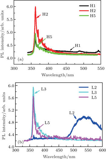
In order to find the reason for the occurrence of high resistivity of LT-grown p-GaN film, the RT PL spectra of all samples are measured and some of them are shown in Figs. 3(a) and 3(b). It is noted that the features of PL spectra for high resistivity (L2) and low resistivity samples (H1, H2, H5, L3, L5) are very different, where a broad yellow luminescence (YL) band centered at 546 nm is present in the spectrum of high resistivity Mg-doped GaN film (L2), whereas only a stronger emission peak centered at 362 nm and a weaker emission peak about 380 nm are observed in PL spectra of samples with low resistivity, i.e., the YL band disappears in these PL spectra. The peak centered at 362 nm is the band-edge emission peak of GaN, the one centered at 380 nm is often ascribed to a free-to-bound Mg transition in lightly Mg-doped GaN,[12,13] and the YL band is related closely to deep level impurities.[14,15] Therefore, the occurrence of YL band in the PL spectrum of sample L2 implies that the compensation mechanisms may come into being in this high resistivity p-GaN film i.e., a large number of compensation impurities may exist in sample L2. In the same way, we are aware that the compensation impurity concentration in the low resistivity sample should be relatively low due to the disappearance of YL band in PL spectrum. On the other hand, it is noted that the variations of PL spectral line for HT-grown and LT-grown p-GaN films with growth condition are also different. PL peak position of HT-grown p-GaN film is nearly unchanged as the NH3 flow rate or pressure increases. However, for the LT-grown p-GaN film, the PL spectral line changes a lot, i.e., the YL band disappears and the band-edge emission peak appears when the NH3 flow rate or reactor pressure increases. It suggests that increasing the NH3 flow rate or reactor pressure may reduce the impurity concentration and improve the crystal quality for LT-grown p-GaN film. We think that the high concentration of compensation impurities in LT p-GaN layer is responsible for its high resistivity, and the variation of the impurity concentration may be the main reason for the variation of resistivity as the growth condition changes.
Fig. 3. Room temperature PL spectra for HT- (a) and LT-grown (b) GaN layers.
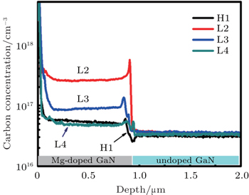
In order to verify our speculation, the depth profiles of unintentionally doped oxygen and carbon concentration of HT- and LT-grown GaN films H1, L2, L3, L5 are checked by SIMS, the oxygen concentration of LT GaN films is nearly equal to the one of H1. However, their carbon concentrations are very different as shown in Fig. 4. The carbon concentrations of H1, L3, and L5 are lower than 1 × 1017 cm−3, much smaller than that in high resistivity p-GaN film (L2). As is well known, carbon is an important unintentionally doped impurity in GaN film grown by MOCVD in which C-contained metalorganic compounds are used as precursors, and several reports have demonstrated that carbon impurity related point defects in p-GaN film may be able to induce YL in PL spectra[16–19] as well as compensate for MgGa acceptors. Therefore, the high carbon concentration should be responsible for the high resistivity of LT-grown p-GaN film. In addition, form the SIMS measurement results, we find that the carbon doping concentration in LT p-GaN film is sensitive to the growth condition, and which decreases with increasing growth temperature, pressure, NH3 flow rate ratio. This result is consistent well with that reported previously.[20,21]
Fig. 4. Depth profiles of carbon concentration for samples H1, L2, L3, L4, measured by SIMS.
However, the carbon concentration of HT-grown p-GaN film is very low compared with that of the LT-grown p-GaN film as shown in Fig. 4, so, carbon impurities may not be the main reason for determining the electric resistivity. The lower carbon concentration in HT-grown p-GaN layer can be due to the fact that more adsorbed hydrogen elements are available from the NH3 and H2 pyrolysis at high temperature, thus facilitating the carbon removal from the surface by converting the methyl groups from TMGa into methane with adsorbed hydrogen.[22] In addition, it can be seen from Fig. 3 that the emission peaks related to carbon impurities are not observed in PL spectra of all HT-grown p-GaN films even though the NH3 flow rate and pressure are both low, suggesting that the carbon concentration in HT-grown p-GaN film may be not sensitive to the growth condition. Both of these two factors may lead to the result that the resistivity of HT p-GaN film keeps nearly a constant when the NH3 flow rate and pressure increase. Therefore, variation behaviors of resistivity for LT- and HT-grown p-GaN films are very different when the NH3 flow rate and pressure increase.
On the other hand, we must keep in mind that nitrogen vacancies (VN) are also able to induce YL band and compensate for MgGa acceptors in Mg-doped GaN film,[23] and their densities may decrease when NH3 flow rate and reactor increases. Thus, they may also result in the different variation behaviors between HT and LT grown p-GaN films.
4. Summary
Two series of p-GaN films with different growth temperatures, i.e., HT 1050 °C and LT 950 °C, are grown by using MOCVD system and the different variation behaviors of resistivity for these two series of p-GaN films are investigated. It is found that the resistivity of LT-grown p-GaN film is more sensitive to the growth condition compared with that of HT-grown p-GaN film. For LT-grown p-GaN film, its resistivity reduces rapidly when the NH3 flow rate or reactor pressure increases. However, it is nearly unchanged for HT-grown p-GaN film. We are aware that the different variations between HT- and LT-grown p-GaN films with growth condition may be attributed to the fact that carbon concentration in LT-grown sample is much higher than that in HT-grown sample and meanwhile it is sensitive to growth conditions of LT-grown sample compared with of HT-grown sample.
Reference
1
NakamuraSFasolG1997The Blue Laser DiodeNew YorkSpringer
Different variation behaviors of resistivity for high-temperature-grown and low-temperature-grown p-GaN films
[Yang Jing1, Zhao De-Gang1, †, , Jiang De-Sheng1, Chen Ping1, Liu Zong-Shun1, Zhu Jian-Jun1, Le Ling-Cong1, Li Xiao-Jing1, He Xiao-Guang1, Zhang Li-Qun2, Yang Hui1, 2]


 , Jiang De-Sheng1, Chen Ping1, Liu Zong-Shun1, Zhu Jian-Jun1, Le Ling-Cong1, Li Xiao-Jing1, He Xiao-Guang1, Zhang Li-Qun2, Yang Hui1, 2]